
Teardown: The BMW / Harman NBT HU Infotainment Unit
Overview


Today’s teardown is of the BMW NBT HU infotainment unit, built by Harman Automotive. This head unit was used between 2012 and 2019 across a wide array of models in BMW’s lineup, in everything from their sedans to SUVs.
It sat in the middle ground of specs and functionality:
The oldest and lowest-end vehicles got the "CIC” Car Infotainment Computer
The middle-ground vehicles got the NBT HU system (the first of the ‘high’-spec systems)
This is the system we’ll be tearing down today
The newest and highest-specification vehicles were outfitted with the NBT EVO HU system (a newer hardware and software variant of the original NBT HU)
For an operating system, the unit runs QNX 6.5.0, released in July 2010. Surprisingly, this was continued even on the NBT EVO HU, which was sold up and through 2019!
The Outside
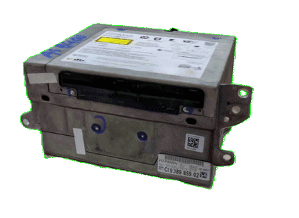
The top of the NBT HU unit, showing the device’s labeling.
The device’s outer casing is made from a surprisingly thick metal. This allows the case to double as the device’s heatsink, that way it doesn’t bake itself alive when buried in the dashboard!
There’s also a lot of interesting information on the label. Most of it is compliance or manufacturing information, but some of it is juicy, like the FCC ID!
Manufacturered By: Harman Automotive
Model: NBT HU
QD ID: B017665
Anatel: 2309-12-2886
TRC/SS/2012/117
ETA: 2211/2012/WRLO
Aprobado CNC C-10873
COFETEL: RCPHANB13-0027
27390/SDPPI/2012
FCC ID: T8GB067
IC: 6434A-B067
OMAN-TRA
TRA/TA-R/0557/12
02/05/2012
TRA
REGISTERED No: ER0086285/12
DEALER No: 0014517/08
NTC Type Approved
No. ESD-1206229C
ICASA
TA-2012/723
APPROVED
It’s also worth taking a peek at the front sticker of the unit to get a bit more data about which specific variant of the module this is.
The label located on the front of the NBT HU.
The front sticker contains the following information:
Manufactured in the USA by Harman Automotive
Model No: HB B114 EC 540
250382 10 HW 31 SNR 2662205
B114540E3299839
S-ID XXXXXXXXXXXX
MAC-Adr 9cdf03a51714
BT-Adr 9cdf03cfd010
Accession No 1331416-000
Version US
Date 32/14
Type: NBT HU
CE 0682
BMW 6512 CI936576701
The final number listed can be converted into the part number - remove the “CI” prefix and “01” suffix and you’re left with “9365767”. Add the BMW prefix 6512 to the front, and you come up with a part number of: 65129365767
According to RealOEM, this specific variant of the head unit was used from 07/01/2014 through 10/06/2016.

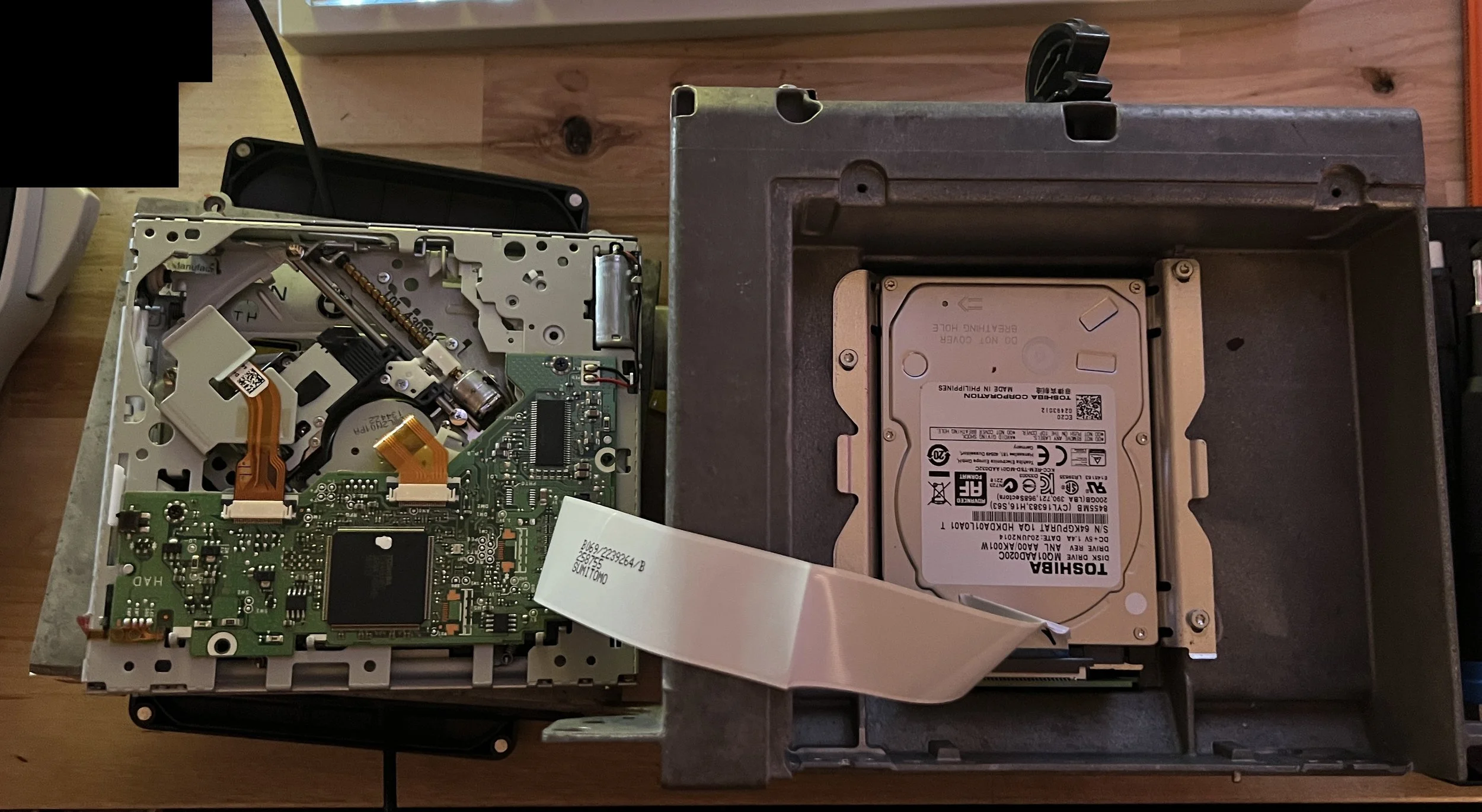
The top cover lifts off to reveal the unit’s disk drive. When lifted, this exposes the unit’s hard drive, to which the disk drive is connected via a ribbon cable.
The Toshiba 200GB HDD removed from the NBT HU device.
This hard drive holds the unit’s navigation data and map files, among other miscellaneous system files. These drives are also protected via an ATA-password, making them quite difficult to access or replace!
These HDDs have been known to die, after 10+ years baking in the dashboard.. luckily, the aftermarket has come up with a few interesting solutions to allow for the unlocking and replacement of these drives.
The unit showing an empty upper tray, with the HDD removed and disk drive disconnected.
Under the HDD, there isn’t much - in the above photo, I disconnected the disk drive from the daughter board, and then unplugged the HDD. All that’s exposed are the two tiny daughter board connectors, and nothing else!
The Inside
The NBT HU unit with the top cover removed, exposing multiple PCBs and device components.
Our first peek at the inside of the unit! As you can tell, the device is made up of quite a few PCBs and components. The black shroud on the right is the device’s fan, and the vertical card on the left holds most of the radio transceivers - SDARS, AM, FM, and GPS (or if you’re in the UK, I believe the DAB connectors are on this card).
Towards the back you can see the back panel connector PCB (shielded in metal), which is the spot where the vehicle’s wiring harness connects to the unit. The black fiber optic lines you see running across the PCB are carrying the module’s MOST bus connection.
Identifying the Layers
Because of the device’s complicated multi-PCB construction, I thought it would be productive to deconstruct the device and identify each of the layers first.
A deconstruction of the BMW NBT HU, identifying the various PCB layers.
To simplify talking about the construction of the device, I’ve divided it into four separate main PCBs:
Layer 0
This is the bottom-most PCB, featuring the XILINX SPARTAN-6
Layer 1
This is the upper PCB, featuring the ATMEL MEGA169P
RF PCB
This is the PCB which holds most of the device’s radio frequency transceivers and connectors (SDARS, AM, FM, GPS, DAB)
Harness PCB
This is the rear PCB which facilitates the main wiring harness connection.
Note, this is not a list of all of the device’s PCBs - instead, it is just the main ones… there is also the HDD connector board, the SoC daughterboard installed on the underside of the Layer 0 PCB, and the CD-ROM drive’s controller PCB.
The RF PCB
The NBT HU’s RF PCB, as seen from the outside.
Starting from the top and working our way down, the easiest PCB to start with is the RF (Radio Frequency) PCB.
RF PCB - Model Number
At the top of the board, my variant features the following model number(?)/information on the silkscreen:
2357828 12JB
B073 4065 LS
RF PCB - Rear Connectors
The PCB I’m working with has three connectors installed - pink, white, and black - though up to four can be used depending on the region.
Pink Connector: SDARS (USA)
White Connector: FM2 Radio
Black Connector: AM Radio
A photo of the European version of the RF module, showing the curry and green-colored DAB connectors (photo taken from device’s FCC listing)
In other regions, the pink connector on the RF PCB is replaced by a green connector, and another connector is added above.
“Curry” Connector: DAB III (Europe Only)
Green Connector: DAB L (Europe Only)
RF PCB - Components and ICs
To start diving into the components, my variant of the board has two large NXP ICs on the right side, along with some SDRAM.


The specific chips are:
NXP HD Radio SAF3560HV/102
NKR430.00
kSD14101
Described on NXP’s website as a “terrestrial digital radio processor”
Micron DRAM 48LC8M16A2
1418 2-7
P -6A A1T L
Described on Digikey as 128MB of SDRAM
NXP SAF7741HV/125
S1T449.1
ZSD14061
Described on NXP’s website as a “car radio Digital Signal Processor” (DSP)
Unfortunately, the PCB also contained some difficult-to-access ICs. There were three metal shells installed on the PCB - one on the outside, and two on the inside. This is commonly done for Radio Frequency Interference (RFI) and Electro-magnetic Interference (EMI) protection, due to the sensitive radio-related ICs inside.
Two of these covers were relatively easy to pop off, but the third would unfortunately require un-soldering, and I’m trying to keep this unit in working condition (for now…). Hopefully someone could chime in with what this big can is responsible for!
Now then, on to the next PCB.
The Harness PCB
The BMW NBT HU Rear Harness PCB
The harness PCB is the rear-facing PCB on the back of the unit. It’s completely shrouded in metal, likely for structural integrity reasons? (Pushing the harness into place can be quite the ordeal, so I understand why you’d want to give it some extra strength…)
There’s not really anything to see for ICs - this PCB mainly routes power, data, etc. down into other PCBs through the connector at the bottom of the board, and lets the fiber-optic MOST connection pass through down onto the Layer 1 PCB. There are a few capacitors, and two large “VOGT”-labeled transformers…? Inverters…? Honestly, I’m not sure - I couldn’t find any details on them on Google, so they were likely made by a supplier specifically for BMW (or even for this specific part).
Just in case someone else knows what they are, the full text on the red components seems to be:
VOGT E6 200 H 1290.290
Overall, a pretty simple PCB. On to the next one!
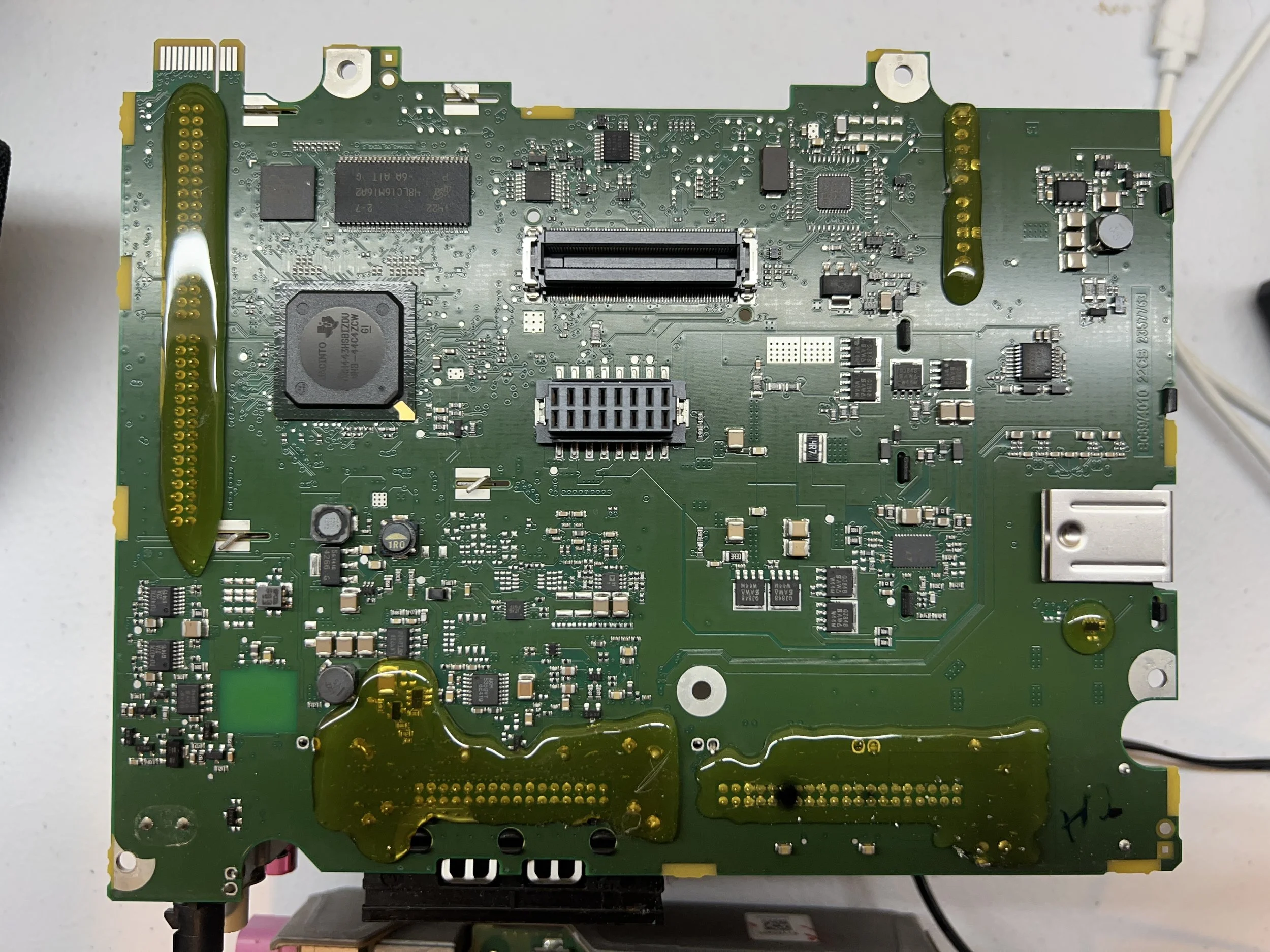
The Layer 1 PCB


Taking a peek down at the device’s upper (Layer 1) PCB, we see a few microcontrollers and major components:
ATMEL MEGA169P-15AT (datasheet)
AKM AK4628AVQ 1341EAA (datasheet)
Analog Devices ADV7180WBST48Z (datasheet)
The ATMEL chip is an “8-bit AVR Microcontroller with 16K bytes in-system”, according to the IC’s datasheet. The AKM chip is a “high performance multi-channel audio codec” - it does analog to digital conversion and back, with 24-bit audio data. And finally, the Analog chip is a “10-bit 4x Oversampling SDTV Video Decoder”. Well, it’s definitely an infotainment system!
Layer 1 PCB - The Underside

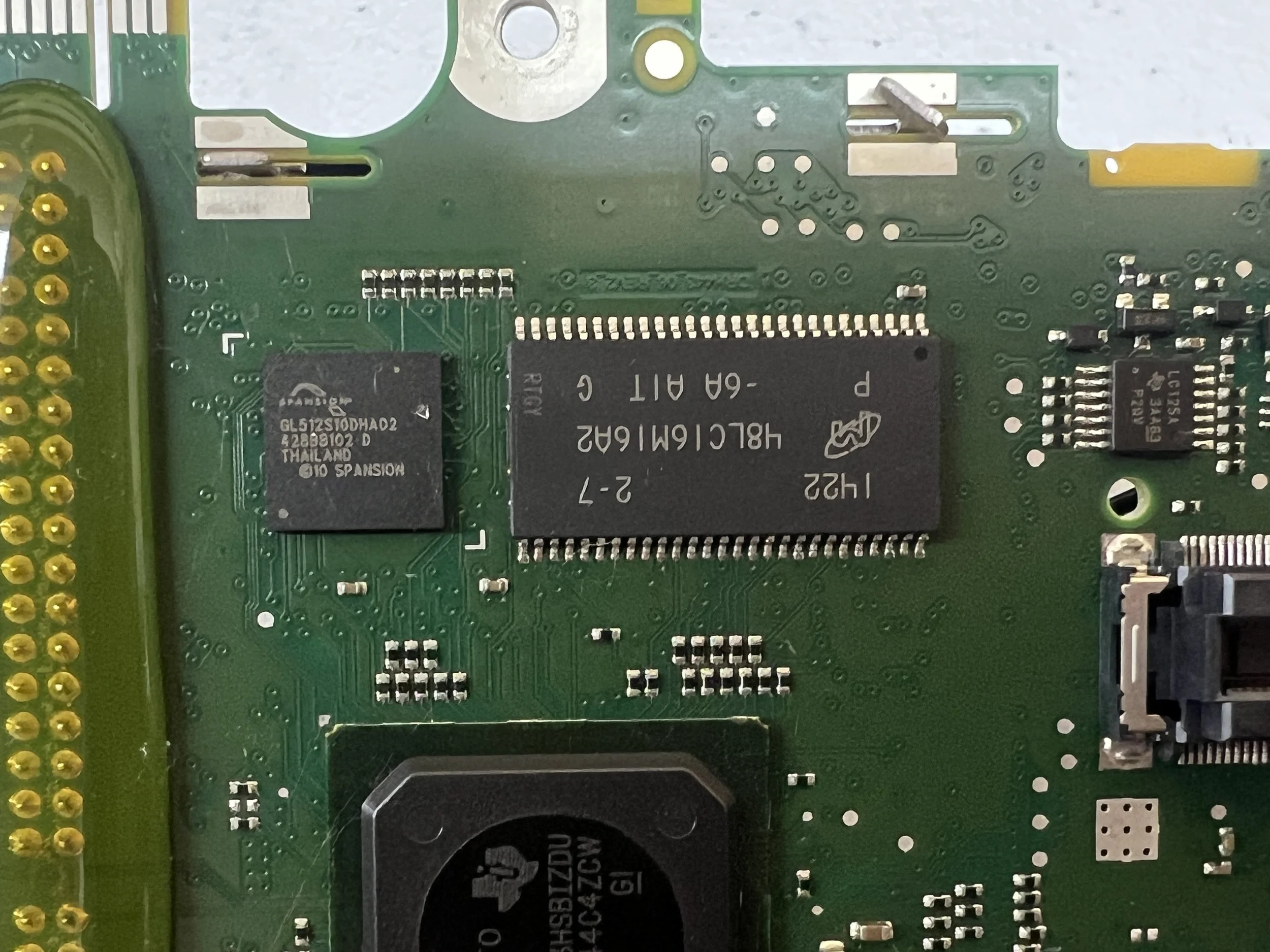

The underside of the Layer 1 PCB also holds a number of interesting components. There’s a TI Jacinto processor, some Micron SDRAM, and a few connectors that allow the board to socket into the Layer 0 PCB. The specific ICs are:
TI Jacinto DRH443HSBIZDU
SNB-44C4ZCW GI
Note, this also might be “$NB-44C4ZCW GI” - it’s hard to tell if it’s a dollar sign…
Micron 48LC16M16A2
1422 2-7
P -6A A1T G
According to the Micron website, this is 256MB of SDRAM
The Layer 0 PCB

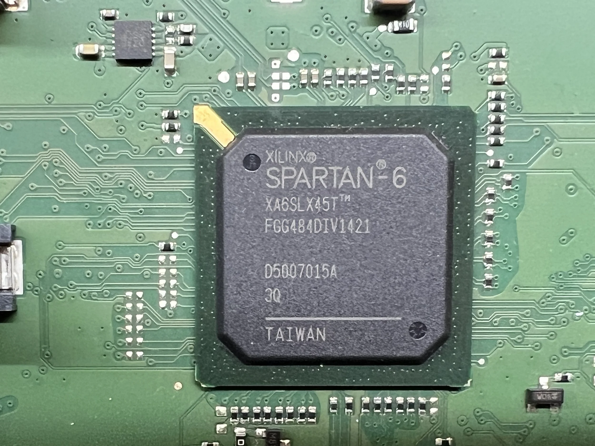


Last but not least, we have the Layer 0 PCB - the bottom-most PCB in the NBT HU. This board has a number of interesting components, both the front and backside are packed full of cool ICs. The main components on the top side of the board are:
XILINX SPARTAN-6
XA6SLX45T
FGG484DIV1421
D5007015A 3Q
According to the datasheet, this is a Xilinx Automotive (XA) Spartan 6 FPGA.
ublox UBX-G6000-BA
B0600
00930054
1422A3
According to the datasheet, this is an automotive-grade GPS chip from u-blox.
ST M29W400FT
5AZA6
99A0Q VS
MYS 99 415
From what I’ve found, this technology is a mix of Numonyx, Micron, and ST. The relevant datasheet seems to be here.
This IC is listed as 4-Mbit Boot Block 3V-supply Flash Memory
Next, there are three different sockets on this side of the PCB. Two are for connecting to the Layer 1 PCB, and one (the one closer to the edge) is for connecting to the external HDD (for loading map data, user preferences, etc).
Layer 0 PCB - The Underside


The underside of the Layer 0 PCB has quite a few things going on. The left side of the board contains an SoC daughterboard that has the PCB’s main processor installed on it. This modular setup is installed in an edge connector socket, allowing the board to lay flat against the Layer 0 PCB.
For major ICs, the Layer 0 PCB itself has two:
NVIDIA18E4B180 1415A3
S TAIWAN
NMA195 S03
GF-EMP9S-A-A3
This seems to be an NVIDIA EMP9-series GPU, but I can’t find any trustworthy documentation about it online…
inova Semiconductors APIX 2
INAP375T
40003_1415
According to the inova website and associated Wikipedia article, this is an “Automotive Pixel Link” (APIX) chip for interconnecting displays and control units, supporting the efficient transfer of video data.
On the topic of the NVIDIA GPU: From doing a bit of Googling, I haven’t been able to find anything regarding the “EMP9” series of GPU that it allegedly belongs to. There are some used and new ICs available, and even solder templates on websites like AliExpress, but nothing even hinting at documentation. That being said, not all hope is lost:
The OEM NVIDIA “nvflash.exe” tool, as captured by the Hybrid Analysis website.
Funny enough, there seems to be a proprietary Nvidia OEM flashing tool called “nvflash.exe” whose strings were leaked by the platform Hybrid Analysis a number of years back, as part of a VirusTotal-style malware scan. The tool contained the strings “EMP9 BIOS based on E566” and “EMP9S BIOS based on E566”. I did some additional searching for “NVIDIA E566”, but unfortunately also ran into a dead end… it’s likely the naming scheme for some sort of OEM embedded GPU chipset, I’d guess.
That being said, if anyone wants to do some additional research and figure out the details on the chip, the nvflash tool and E566 strings could be a good starting place!
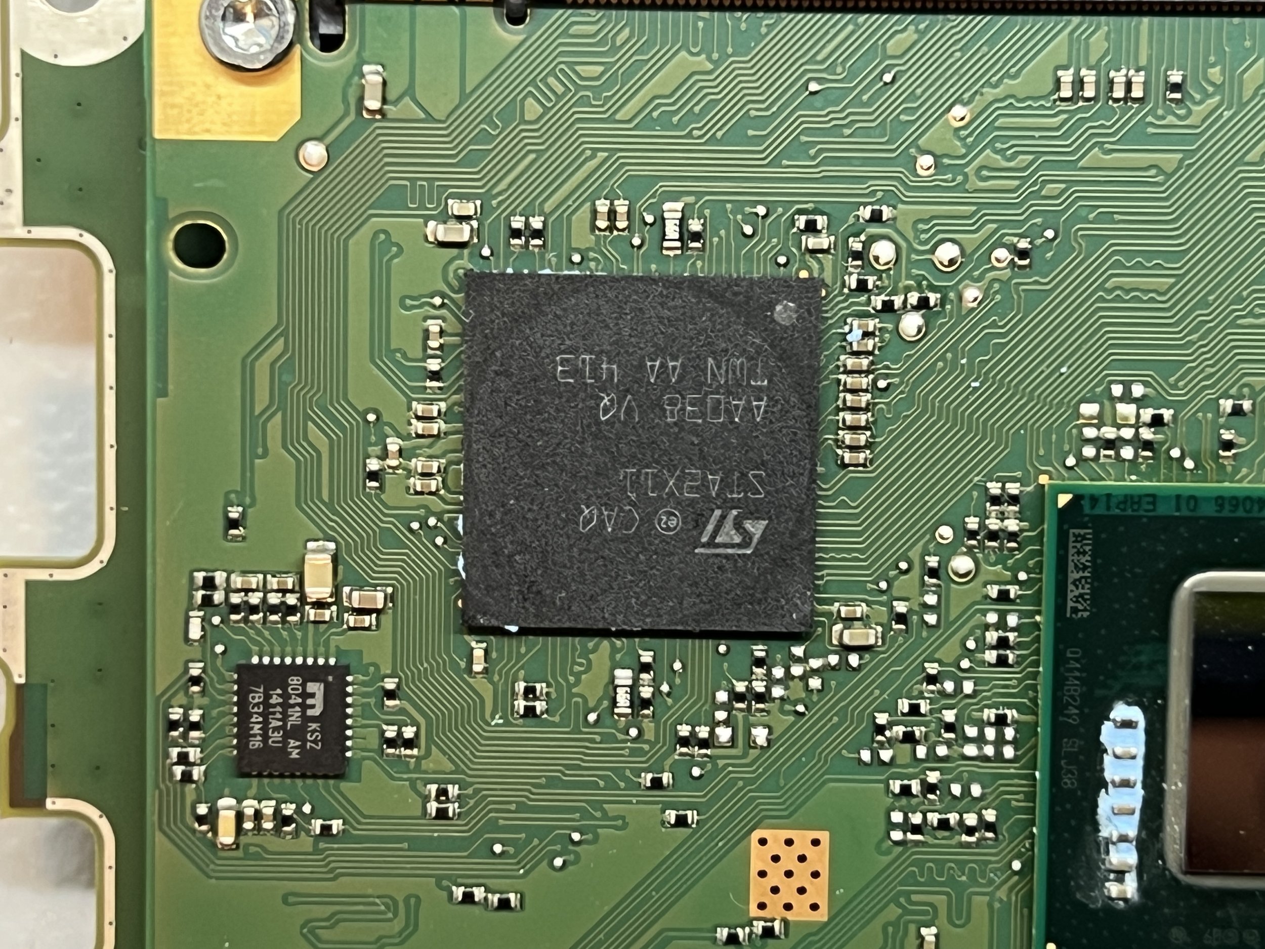
Layer 0 PCB - The Intel Atom Daughter Board


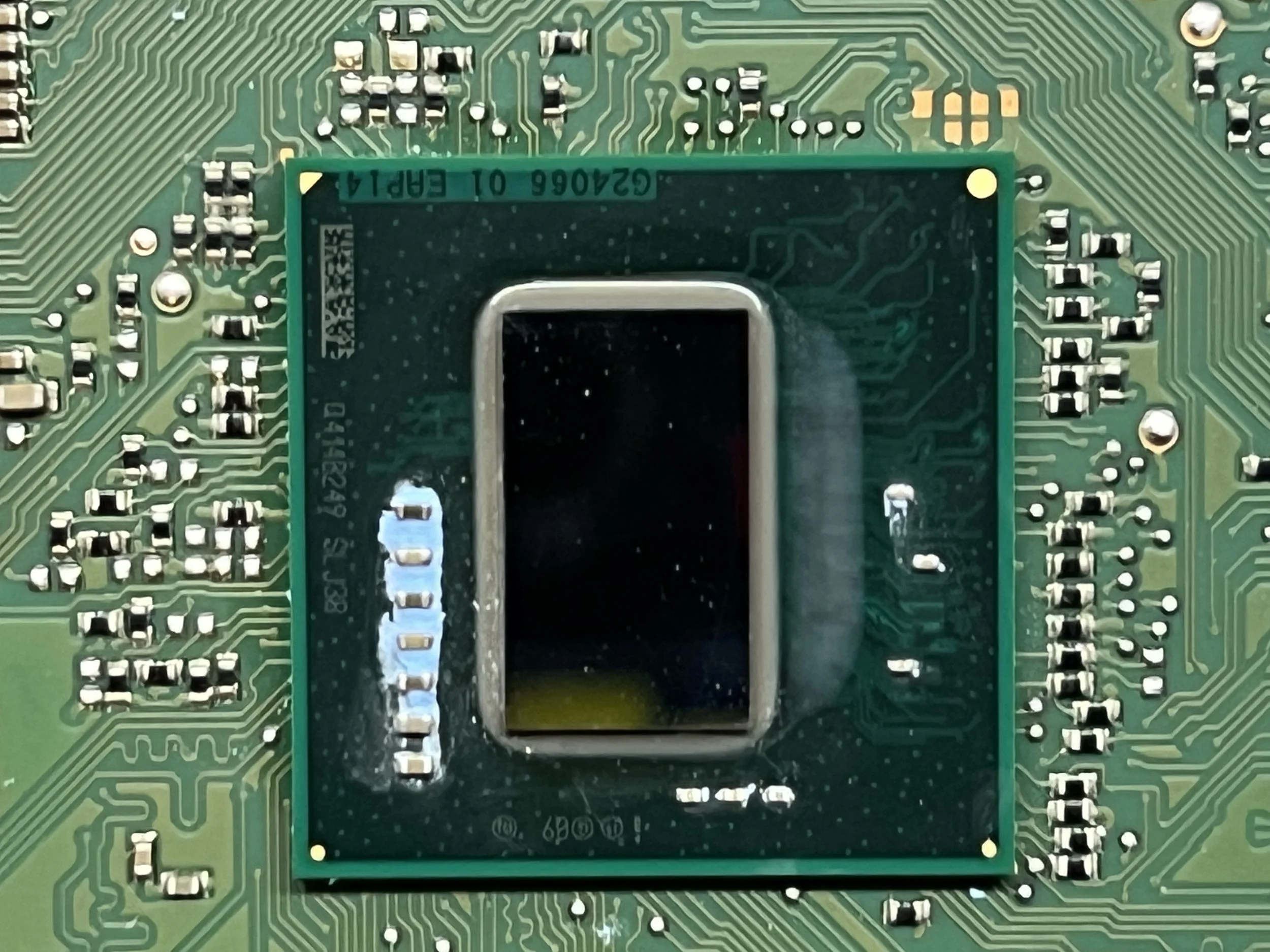
The daughter board that slots into the underside of the Layer 0 PCB can be thought of as the main brains of the device. This processor takes the brunt of the device’s processing needs, and exists as a daughterboard that can is easily removable and replaceable from the Layer 0 PCB.
My board has the following identifier on the silkscreen:
B070 4022 21ED
2512742
HARMAN Automotive
There are two main ICs of note on this board:
Intel G24066 01 EAP14
Q414B249 SLJ38
From what I can find online, the SLJ38 is an Intel Atom processor running at 1.3 GHz.
ST CAQ STA2X11
AA038 VQ
TWN AA 413
While I can’t find any direct documentation, this appears to be an ST ConneXt PCIe IO hub for the Intel Atom
Due to the chips on this board all being Intel Atom related, I would be curious to know if this is simply an Intel Atom reference board design/IP block that Harman purchased and decided to use in its entirety, hence the daughter board design? Not sure!
Daughter Board Security & Modification
From the security side of things, this board also has some interesting quirks: I’ve found examples online of an eMMC jig specifically created to attach to the pins on the edge of this daughter board, allowing you to dump or even re-write the contents of the board’s eMMC flash.
A photo showing an eMMC dumping jig attached to an NBT HU daughter board PCB
The company that makes it has a fun video demonstrating how to hook it up to another Harman board design, instead out of a Mercedes Benz W222: https://www.youtube.com/watch?v=gCd5SfkXHpc
Layer 0 PCB - Rear I/O
A diagram explaining the rear I/O of the NBT HU’s Layer 0 PCB
Before wrapping up the Layer 0 PCB, it’s important we touch on the rear I/O!
There are seven total connectors on my variant of the Layer 0 PCB. Their uses are as follows:
Blue - GPS aerial, color code blue
Burgundy - WLAN aerial, color code burgundy
Beige - USB1 connection (AUX-in USB socket in the center console), color code beige
Curry - USB2 connection (customer smartphone via telephone base plate), color code curry
Light Green - USB3 connection (Telematics Communication Box (TCB)), color code light green
Beige - Bluetooth aerial, color code beige
Pink/Violet - APIX connection and voltage supply to the central information display (head unit screen), color code violet
I included a diagram I made of each of the connections above, but it honestly embeds horribly in Squarespace. Not a huge fan of Squarespace as a blog host…
Conclusion?
Well, there’s not much of a conclusion to be had - I enjoyed tearing down this module and analyzing all of the different portions, and I’m excited to dive into the firmware side of things next. If you have any specific questions about the module or any of the ICs that I didn’t call out, please feel free to reach out! I’d be happy to chat, or post more about it.
As for the software side of things, I’m hoping to get to that soon… I’d like to do a deep dive into the QNX OS used on Harman’s infotainment units, as I’ve been digging into it for a while now.
As always, thanks for reading - hack the planet!
Appendix
All of the misc. raw data that I couldn’t fit into other sections.
Part Numbers & Mfg Dates
The NBT HU unit was manufactured over a wide array of part numbers. Referencing RealOEM’s database, the full list of part numbers and dates is as follows:
65126826793 (11/01/2016 - Present)
65126826775 (07/01/2016 — 01/20/2017)
65126832273 (03/01/2016 — 08/12/2016)
65126819953 (11/01/2015 — 03/01/2016)
65129389859 (07/01/2015 — 11/17/2015)
65129387568 (03/01/2015 — 07/22/2015)
65129383072 (11/01/2014 — 08/06/2015)
65129365767 (07/01/2014 — 10/06/2016)
65129351682 (03/01/2014 — 08/06/2015)
65129347824 (11/01/2013 — 04/17/2014)
65129327320 (07/01/2013 — 08/09/2017)
65129318752 (03/01/2013 — 10/05/2016)
65129315631 (03/01/2013 — 05/21/2013)
65129311073 (03/01/2013 — 06/08/2013)
65129311041 (11/01/2012 — 05/21/2013)
65129308464 (11/01/2012 — 09/19/2012)
65129292442 (11/01/2012 — 08/14/2012)
65129290363 (07/01/2012 — 05/21/2013)
65129289873 (07/01/2012 — 05/15/2012)
65129287877 (07/01/2012 — 04/24/2012)
65129281990 (07/01/2012 — 04/15/2012)