
Teardown: The BMW / Harman NBT EVO HU Infotainment Unit (B211)
Overview
Today’s teardown is of the BMW NBT EVO HU, an infotainment unit built by Harman Automotive - sound familiar?
While very similar, this unit is nooot the same as my previous teardown, which went over the older NBT HU infotainment unit. This is the second generation: The NBT EVO HU!
This unit was considered the “top of the line” unit that was available from BMW between 2016 and ~2021 (though technically, one or two models are as new as 2024!).
The unit attaches to the vehicle’s main infotainment display (called the Central Information Display, or CID) and can perform a number of infotainment-related functions:
APIX connectivity to Central Information Display (CID)
APIX connectivity to instrument cluster (“KOMBI”)
WLAN connectivity (2.4GHz WiFi)
Bluetooth connectivity
Satellite Radio connectivity (SDARS / Sirius XM)
Alternatively: DAB Radio connectivity in European markets
USB connectivity
Ethernet connectivity (via "BroadR-Reach”/OABR standard)
For an operating system, the units run QNX 6.5.0. On top of this, BMW runs their “iDrive” suite of applications - the NBT EVO line is capable of running iDrive 4, iDrive 5, or iDrive 6 (also referred to as ID4, ID5, and ID6). The version running on any individual unit largely depends on when it was manufactured.
Basic Specs
Before we dive into the full teardown, we can check out a basic list of the system specs to understand what we’re working with:
Housing Size: 1.5 DIN
Main Processor: TI OMAP 5, operating at 1.5GHz
Network/Audio Processor: TI Jacinto 5, operating at 720MHz
RAM: 2GB (ID4 units), or 4GB (ID5/ID6 units)
GPU: PowerVR SGX544MP2RC3
Overall, it’s a pretty powerful device! Two ARM powerhouses, 4GB of RAM, a dedicated GPU, and it’s all packed into a 1.5 DIN head unit.
The Outside
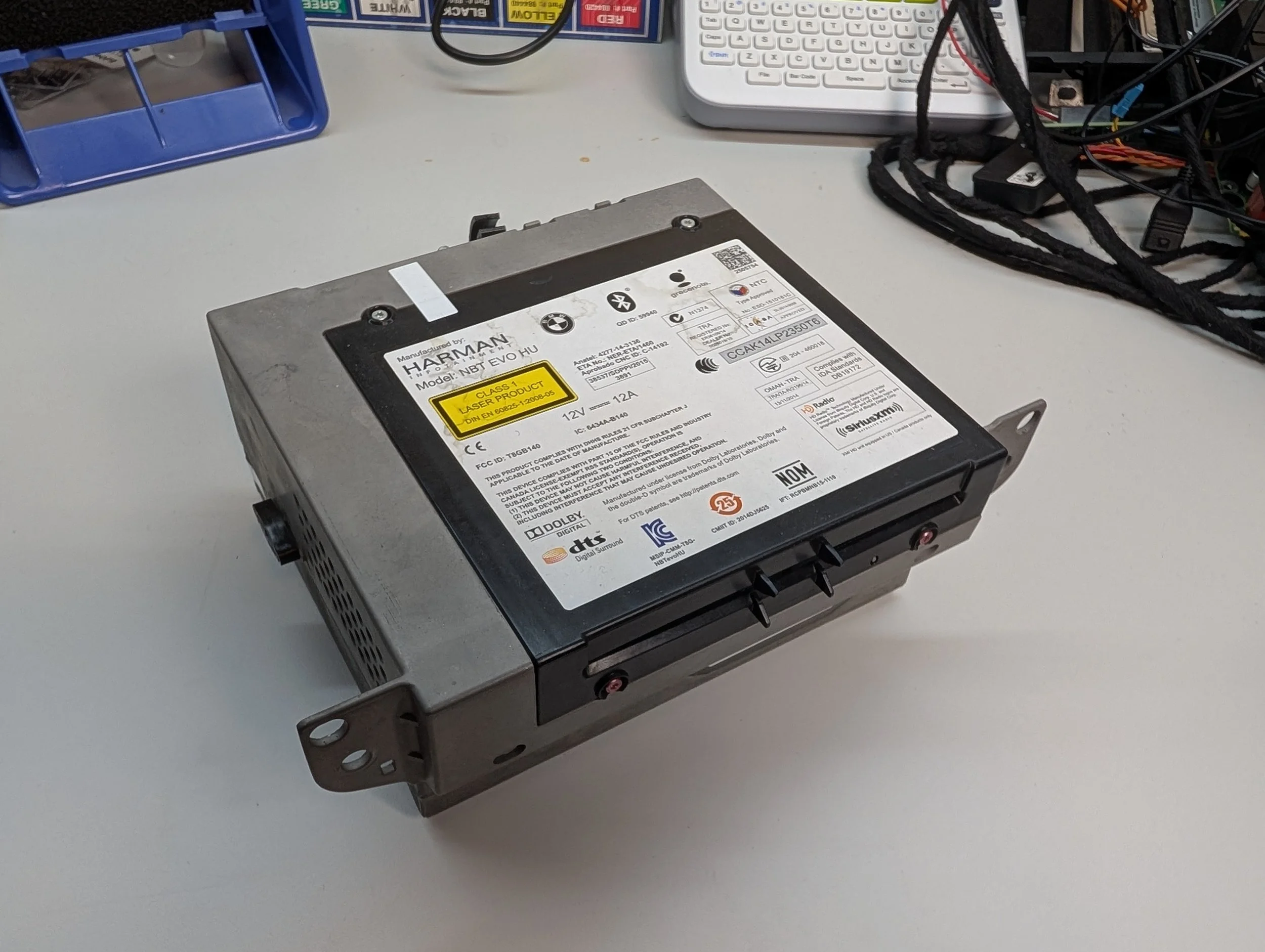


The outside of the unit is very similar to that of the previous generation, the NBT HU. It’s a large metal box - 1.5 DIN in size, to be specific. The disc drive sits on top (the black plastic square with the sticker attached), and all of the device’s I/O is on the rear.
Top Label Information


Zooming in on the label affixed to the top of the device, we get quite a lot of information. I’ll include the full text dump in the appendix of the blog post, but the few most important pieces of information are:
Manufactured by: Harman Infotainment
Model: NBT EVO HU
FCC ID: T8GB140
IC: 6434A-B140
Front Label Information
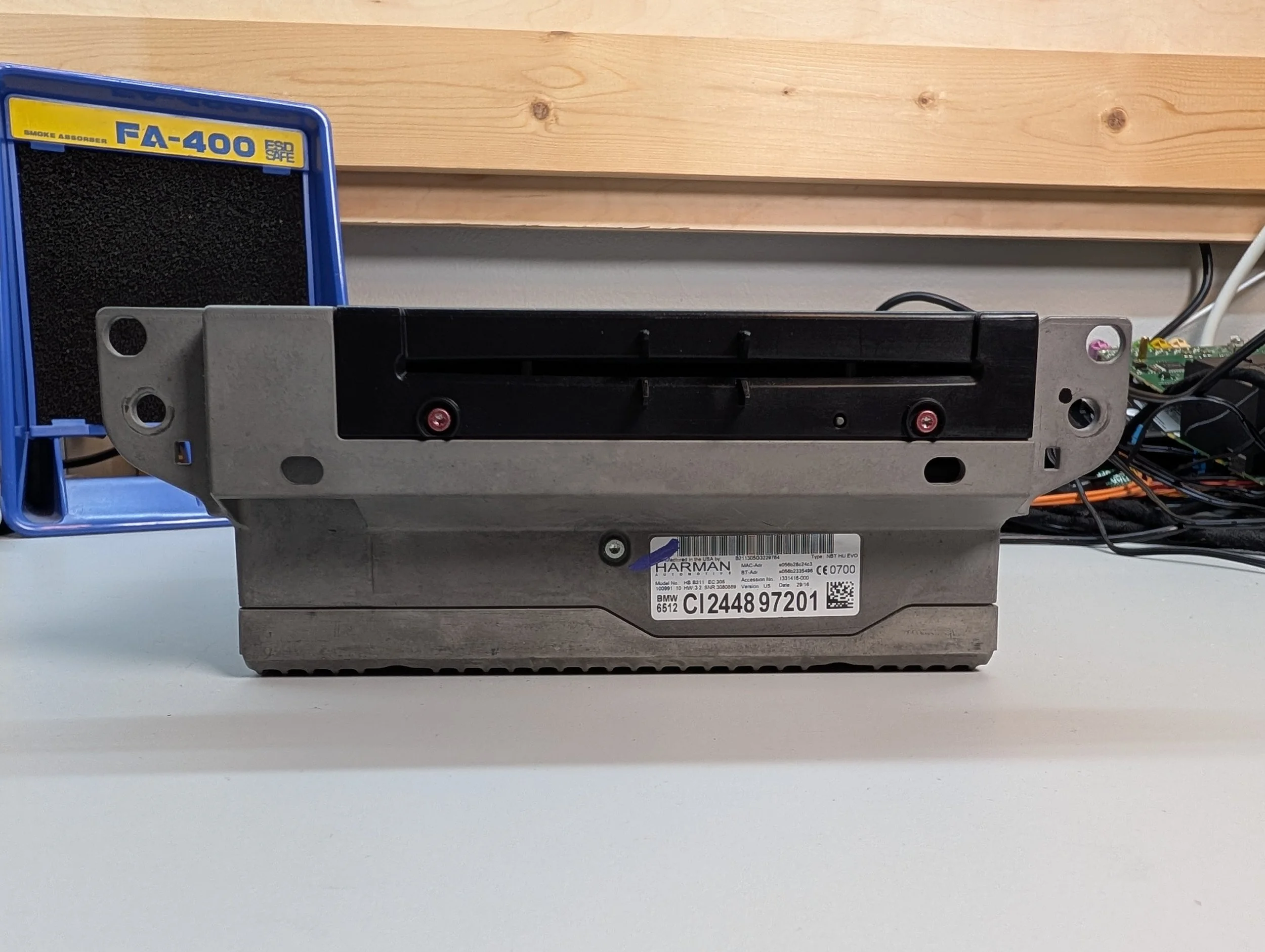

There’s a secondary smaller label affixed to the front of the unit, which has useful information like the production date, part number, specific model variant, and more. As with the top label, I’ll include the full text dump in the Appendix - I’ve included a few of the most relevant pieces of info below:
Model No.: HB B211 EC 305
Date: 29/15
Type: NBT HU EVO
Part Number: BMW 6512 CI244897201
Also, an FYI: The part number listed on the label isn’t quite an actual BMW part number. On any of the NBT-series infotainment units, the front label can be converted to the real part number by stripping the letters from the beginning (making it “244897201”), then stripping the “01” from the end (making it “2448972”), and then prefixing it with “6512”. So: “CI244897201” becomes “65122448972”. Easy!
When faced with BMW part numbers, I usually turn to the website RealOEM. This isn’t sponsored or anything - they just offer free access to the BMW parts catalog, which is 100x easier than having to buy 24 hours of BMW’s TIS subscription for THIRTY TWO DOLLARS USD just to look up a single part number… “right to repair” my ass, they just paywall all of the info.
ANYWAYS - So, plugging this part number into RealOEM, we get the following:
The parts catalog listing shows all of the parts that came before and after this unit.
At the top, you can see the info about our part - so it looks like this particular unit is known as the “Headunit High 2”, and was installed in cars from 2016-07-01 to 2016-08-25.
Under that, the “superseded by” section shows all of the parts that came AFTER our part. These may have been new hardware revisions, new board updates, those kinds of things. And under that, “Supersedes” shows all of the units that came before yours. So unfortunately, we have the second oldest NBT EVO that you can get…
Well, that’s what I get for cheaping out on eBay. On to the disassembly!
Popping the Lid

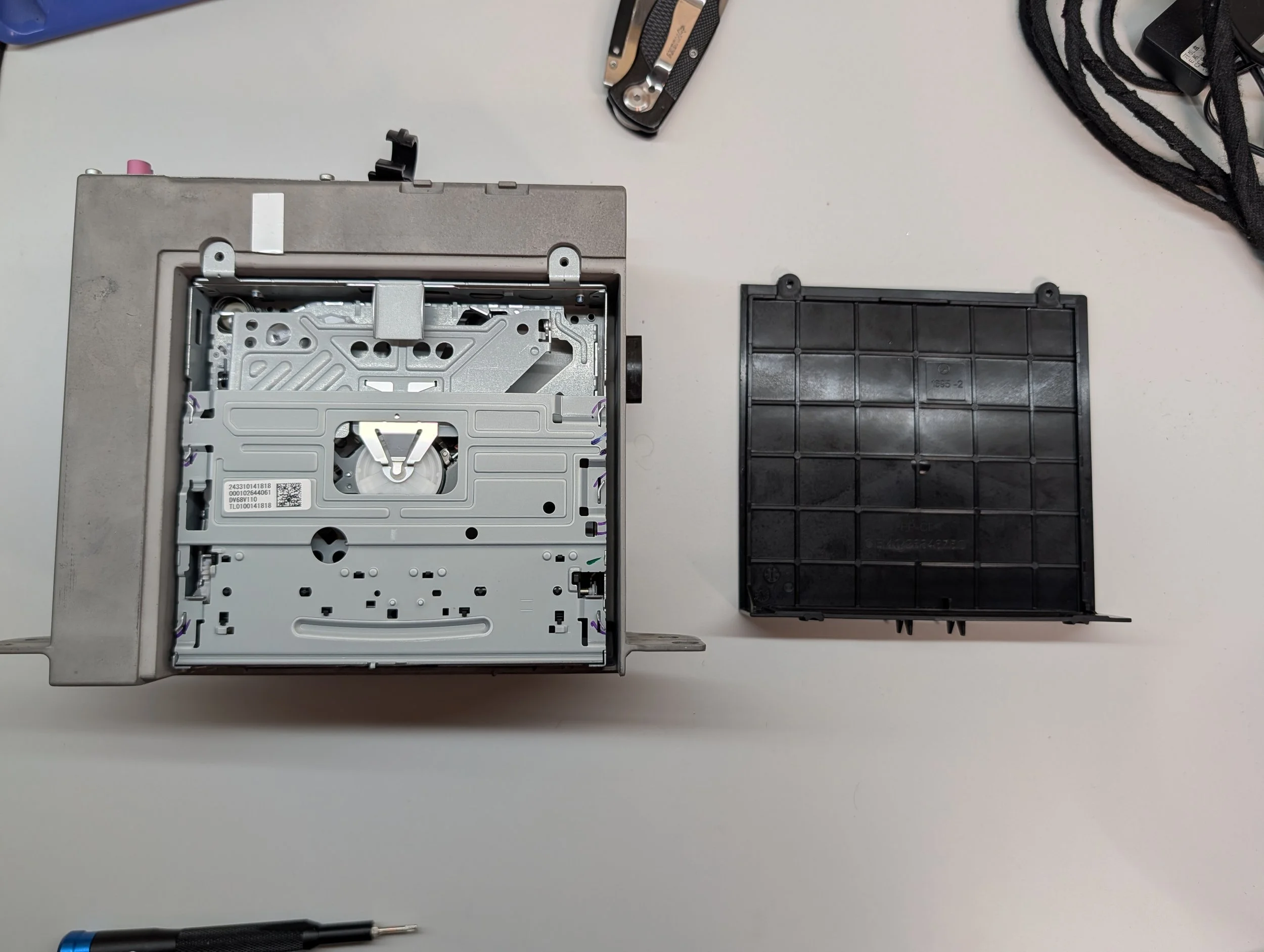
The black lid on top is secured with four screws, and upon removing them, the top of the disc drive is exposed.
A Closer Look at the Disc Drive
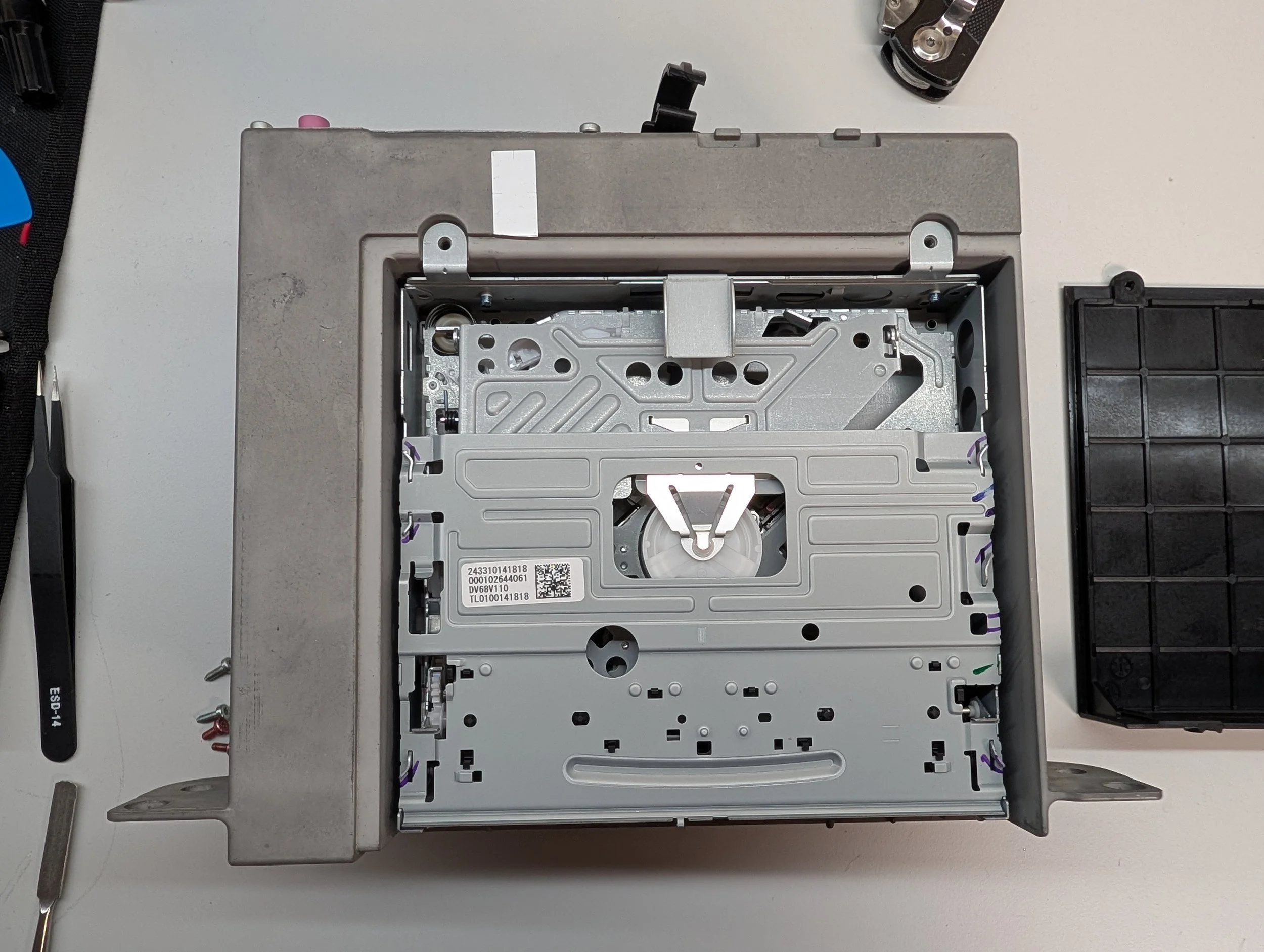


The drive in question is devoid of labels, so it’s hard to say who made it - but the main IC is designed by Panasonic, so that’s where I’ll hedge my bet.
Main Disk Drive IC: Panasonic MNZST9KBAUB 607P402E
Out of all of the info on the small sticker label, the one that garnered the most hits was “DV68V110” - it seems like that’s likely the model number.
The drive is connected to the rest of the unit using a small connector on the underside of the disk drive. This plugs into a small daughterboard that sticks up from the inside of the unit, also providing connectivity to the device’s HDD. Speaking of which…
The Hard Drive


Underneath the disk drive, we get: the device’s hard drive!
This unit features a 200GB Toshiba HDD, model: MQ01AAD020C. It’s connected to the device via a SATA connector that has both SATA data and power.
Upon removing the HDD, we can now see the full contents of the top of the unit - not much else going on here! A small daughterboard with the CD and HDD I/O connectors pokes up from the depths of the unit, but that’s about it… Seems like we’ll have to remove the rest of the screws to continue the teardown.
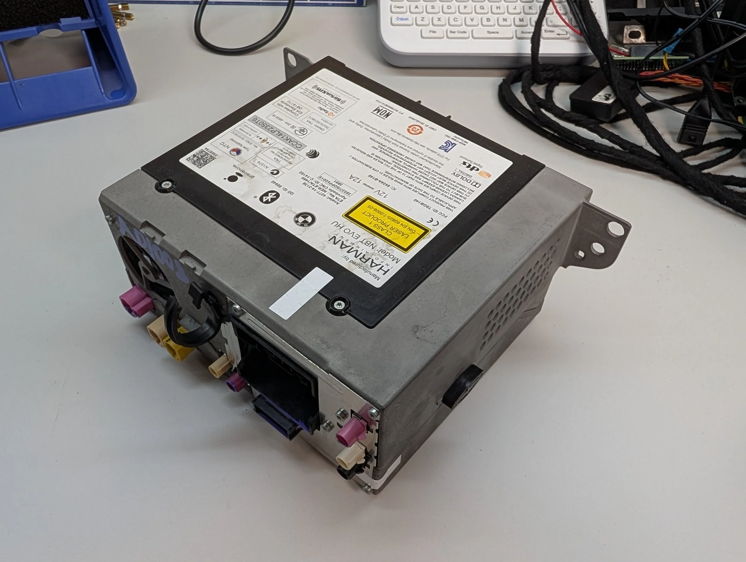
The Back Side


Our last stop before we can start poking around inside the unit: the back side!
There’s a metal plate held on by a few screws that seems to protect and reinforce this section, and happens to hold the two halves of the casing together. Four more screws on the bottom, and the two halves of the casing come apart!
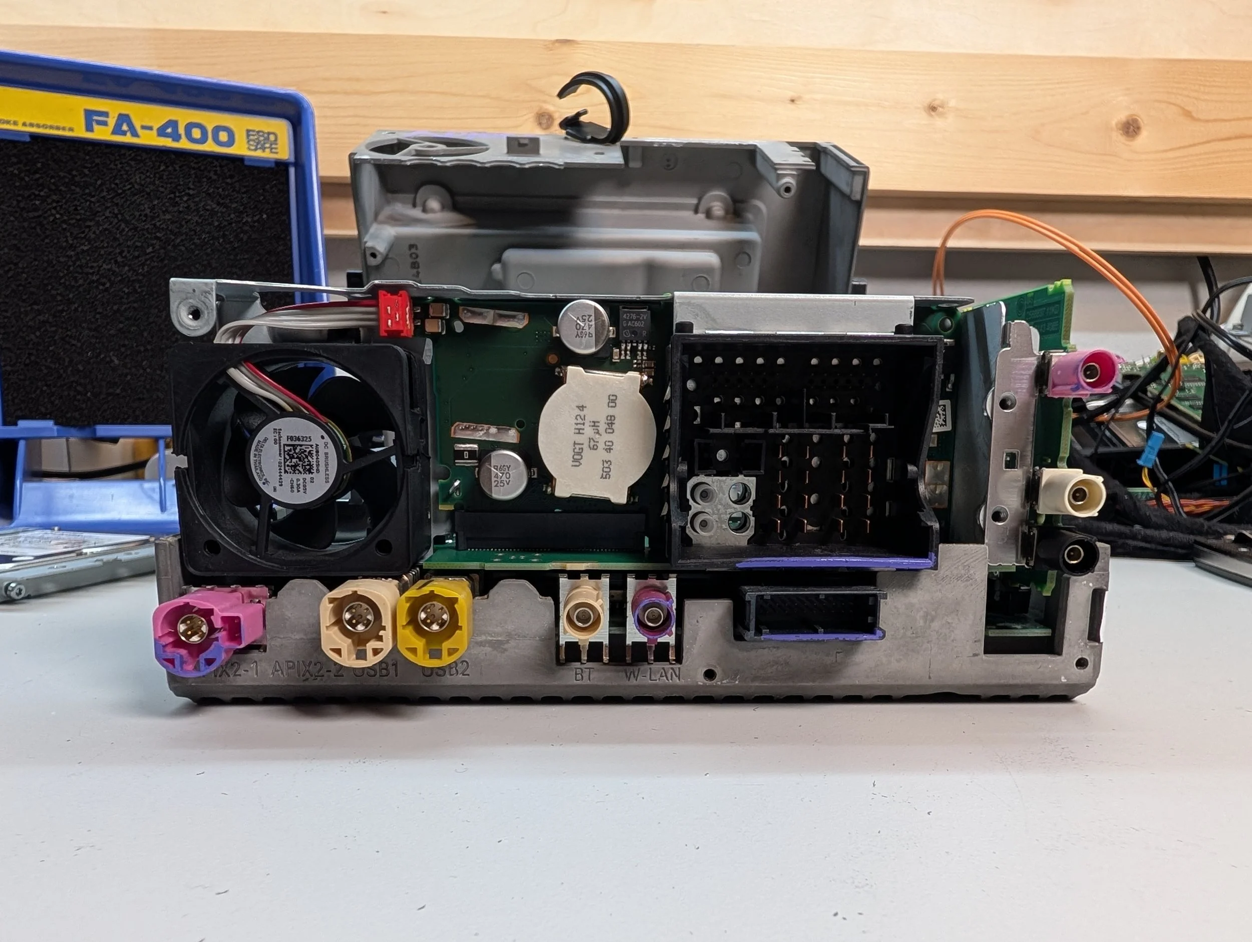
This also gives us the perfect opportunity for a closer look at the rear I/O.
In the center, we’ve got some power supply components, and the Bluetooth and WLAN RF ports.
To the right of those, we have the main harness connector (featuring the MOST fiber-optic connection on the lower left there), and BroadR-Reach Ethernet connector underneath.
Finally, the right side holds our RF card interfaces, which include FM, AM, and SDARS (satellite radio, Sirius XM) on this particular model.
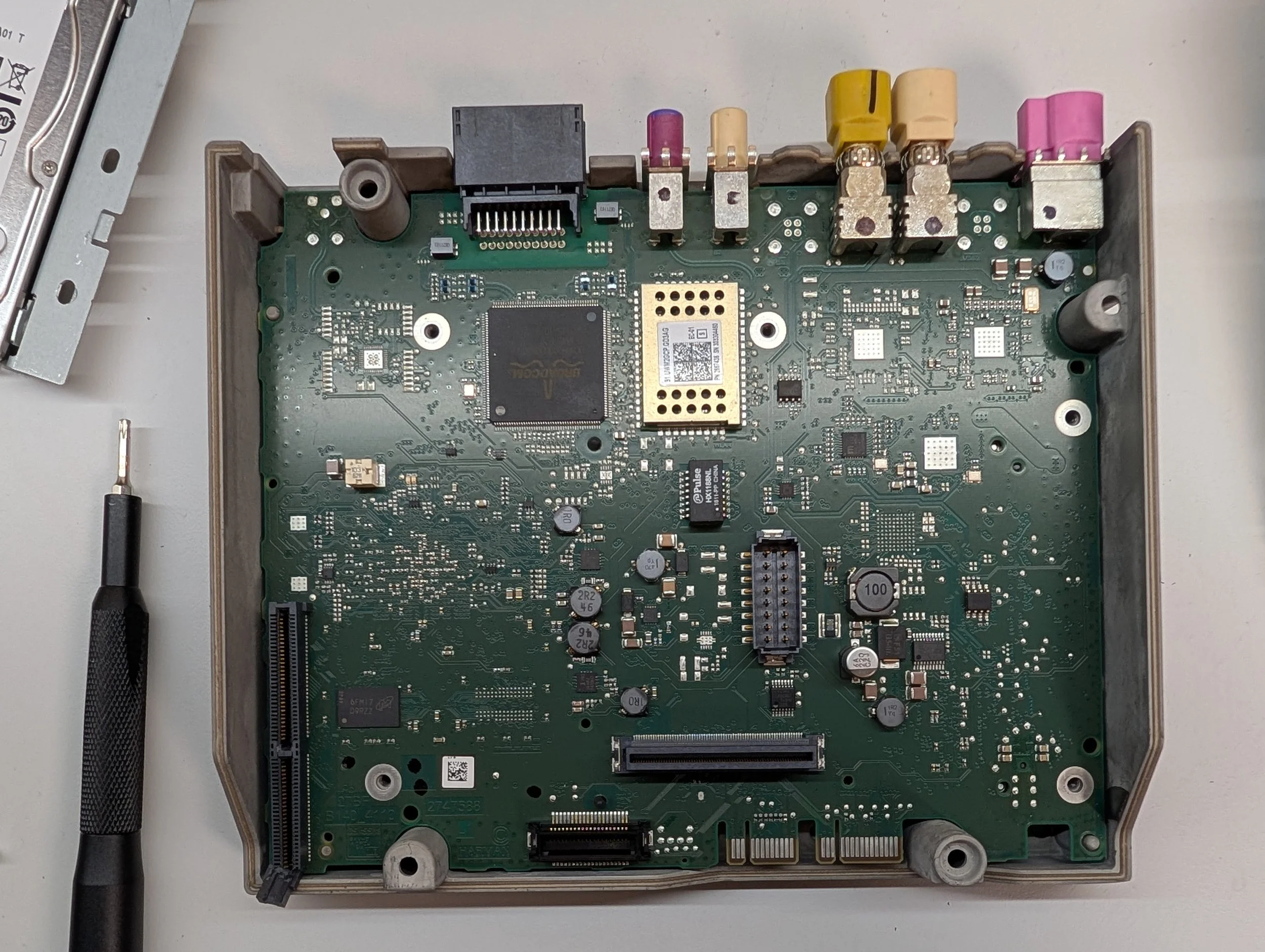
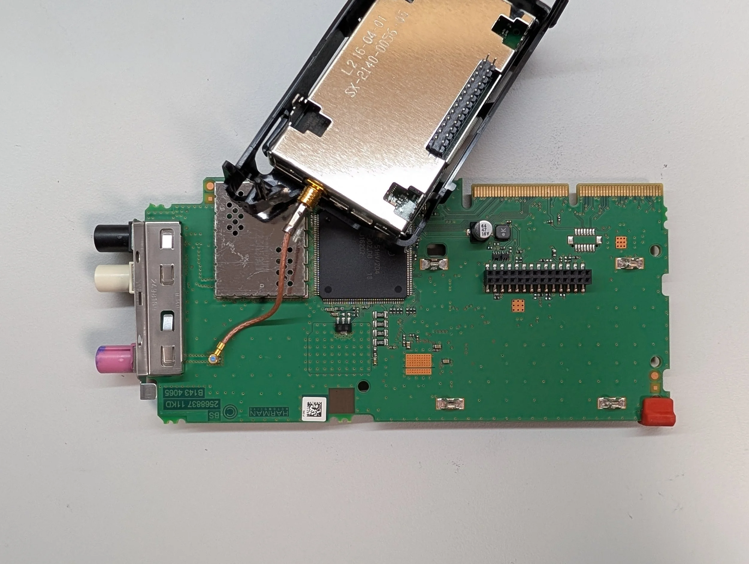
The Inside
Finally, it’s time to poke at the inside of the unit! As with the previous NBT HU teardown, I decided to nickname each of the device’s PCBs to make it easier to discuss them separately.
In total, the device contains ~6 separate PCBs:
Layer 0 PCB (w/ TI Jacinto 5 processor)
Daughter Board (w/ TI OMAP processor)
Layer 1 PCB (w/ Renesas V850 processor)
RF Card PCB (w/ NXP RF Transceivers)
Harness PCB (w/ main wiring harness connector)
HDD/CD PCB (w/ connections to HDD and disk drive)
I’ve included labeled photos of each of these PCBs below. The only one I don’t have a great photo of is the harness PCB, as it’s buried under a whole lot of shielding, and I haven’t had any reason to remove mine yet.
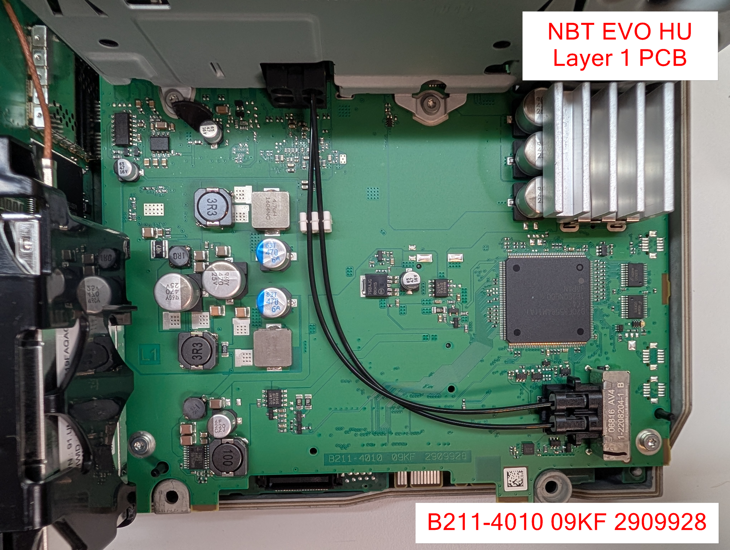


Layer 1 PCB
Board Markings: B211-4010 09KF 2909928
The upper-most layer of the device is the “Layer 1” PCB. This board could be thought of as one of the main interfaces to the vehicle. It holds the harness PCB, which allows for all of the I/O functionality throughout the vehicle’s many buses!
The Renesas RH850 processor found on the top side of the Layer 1 PCB.
In this type of infotainment architecture, the large V850 processor on the top side of the board is responsible for most of the I/O operations with the vehicle itself (CAN, MOST, etc.). It contains the actual CAN, MOST, etc. transceiver logic, and it then communicates the data back-and-forth with the main Application Processor (AP) via a serial protocol like SPI, I2C, etc.
(Actually, a quick reverse engineering note: I’m pretty sure the V850 and OMAP communicate via SPI on this device, since there’s a file called ‘io-ipc-o5.cfg’ on the OMAP board that contains some of the SPI-specific IPC configuration lol. But I haven’t confirmed that 100%, just an interesting side note)
Major Components - Layer 1 PCB (Top side)

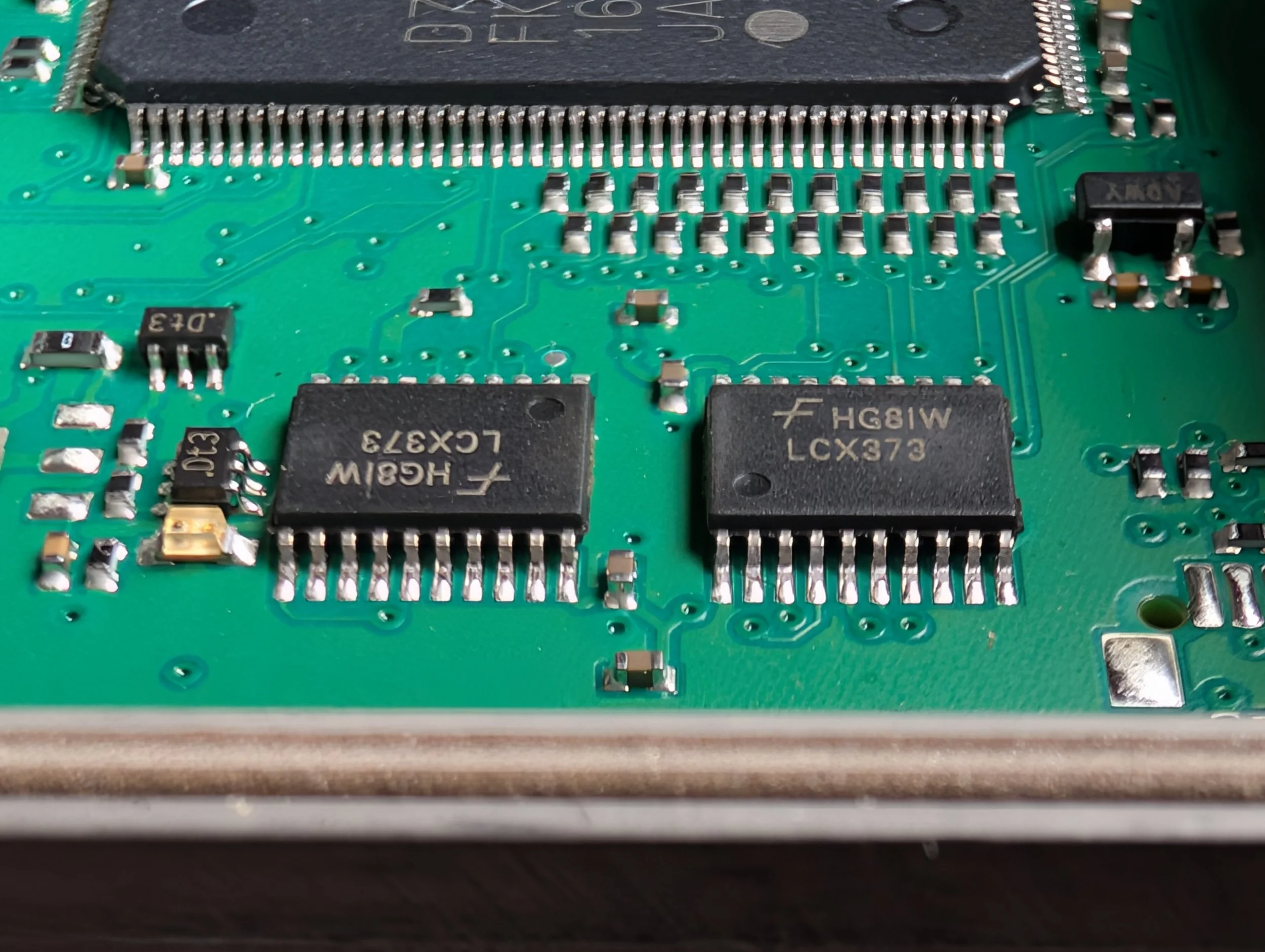
Rensas V850 Microcontroller (datasheet)
D70F3558AM1(A)
FK4 1625QNE00 JAPAN
NXP High-speed CAN Transceiver (datasheet)
TJA1043T T6000051 THD16161
Fairchild Low Voltage Octal Transparent Latch (similar-ish datasheet?)
HG81W LCX373
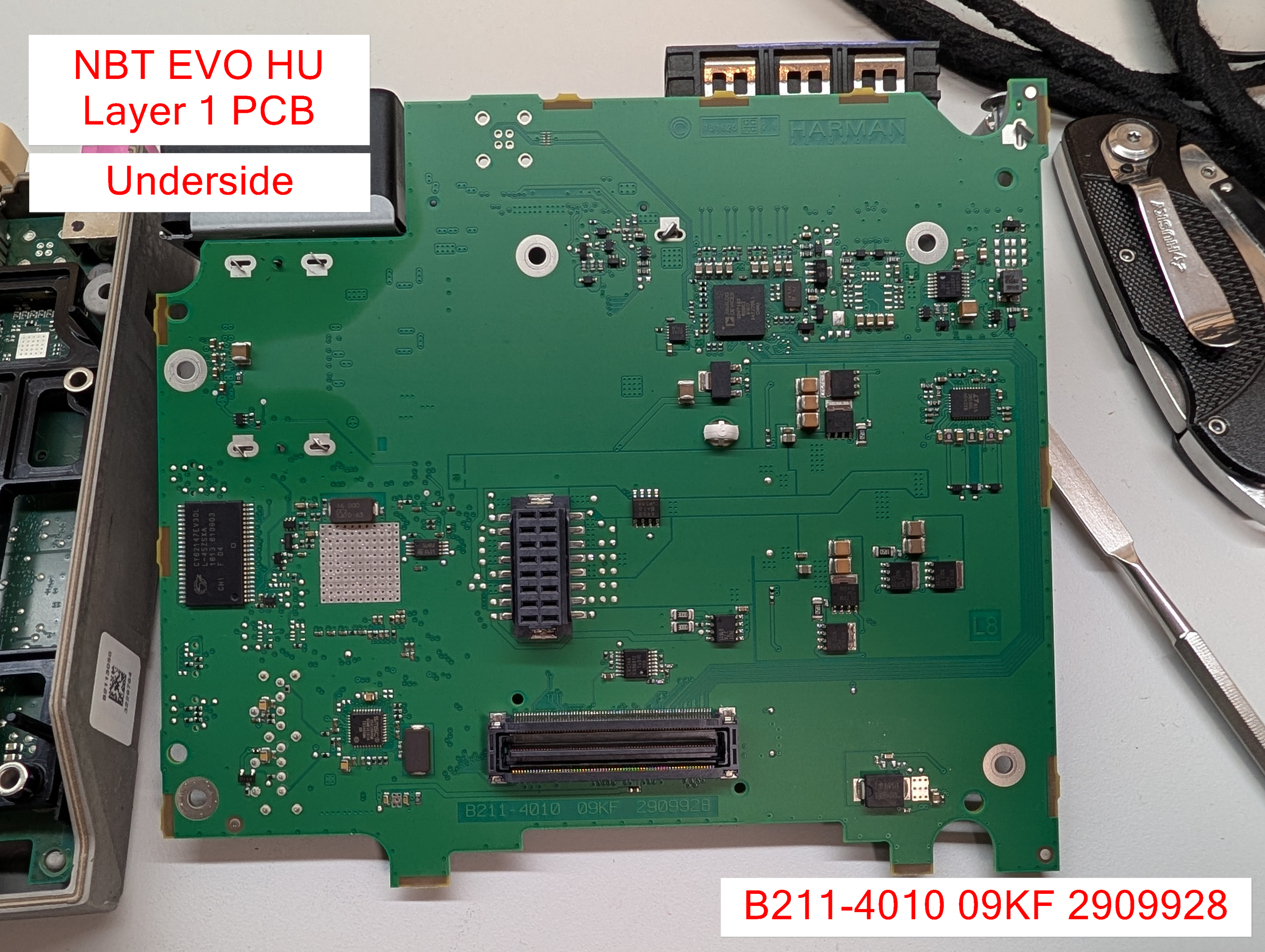
The Underside of Layer 1
The underside of the Layer 1 PCB.
The underside of the Layer 1 PCB features two large connectors that allow for data transfer with the Layer 0 PCB and it’s associated processors.
Major Components - Layer 1 PCB (Underside)
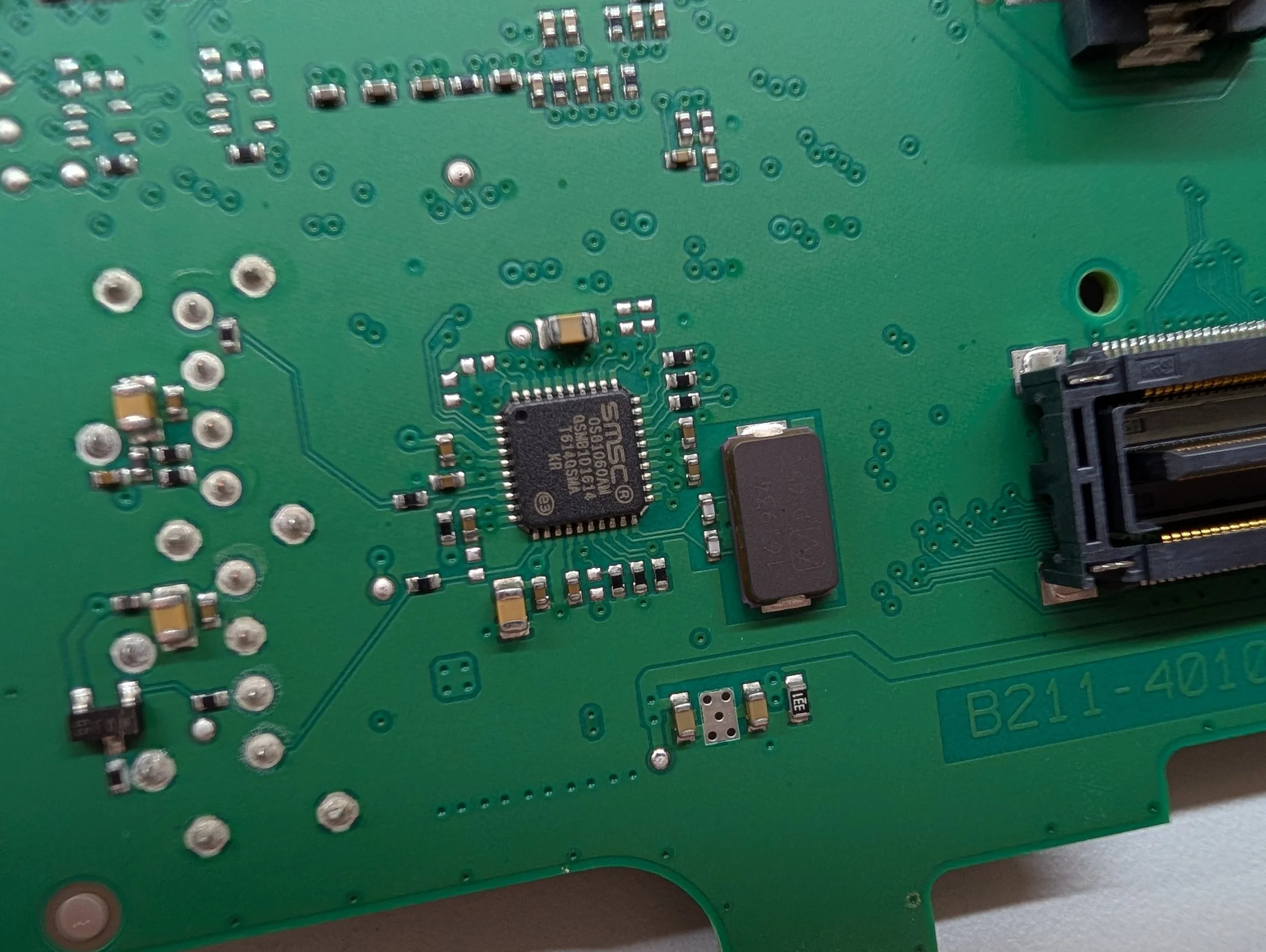
Analog Devices Integrated Video Decoder and HDMI Receiver (similar datasheet)
ADV7483 WBBCZ #1617
3472286.1 CHINA
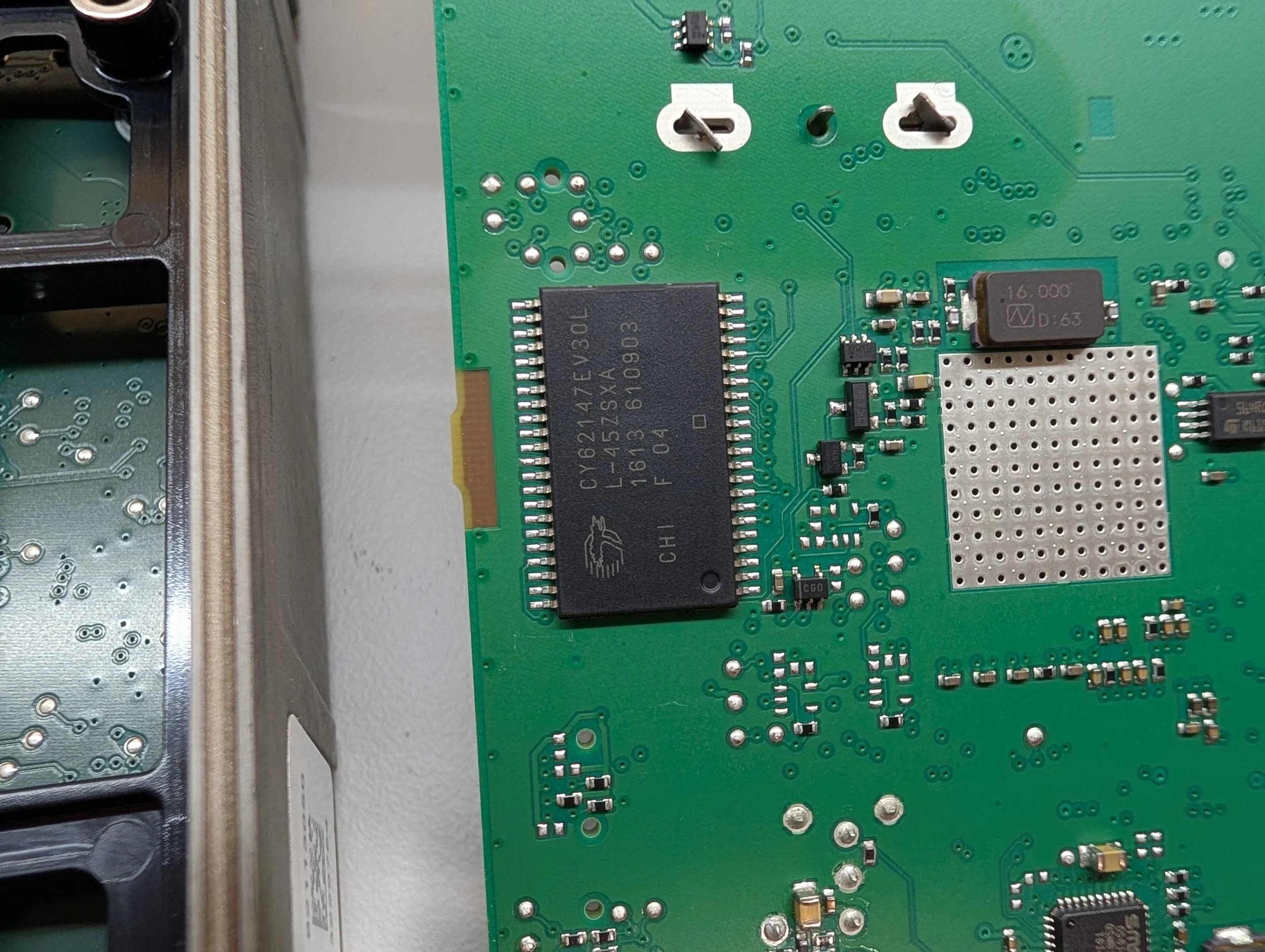
Cypress/Infineon 4-Mbit Static RAM (datasheet)
CY62147EV30L L-45ZSXI
1613 610903 F 04
SMSC MOST25 Intelligent Network Interface Controller (similar datasheet)
SMSC OS81060AM
QSMB101614 T614QSMA KR
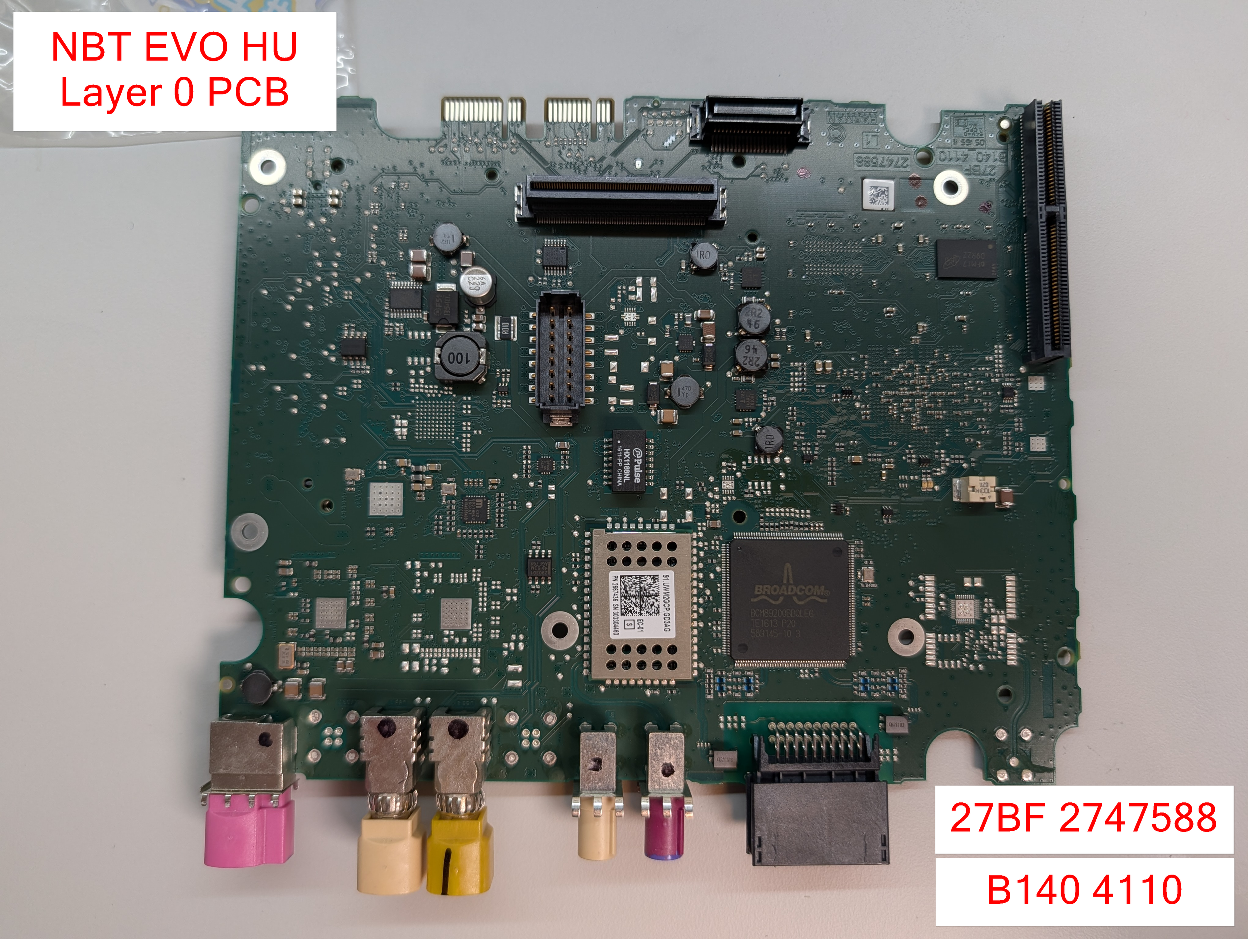
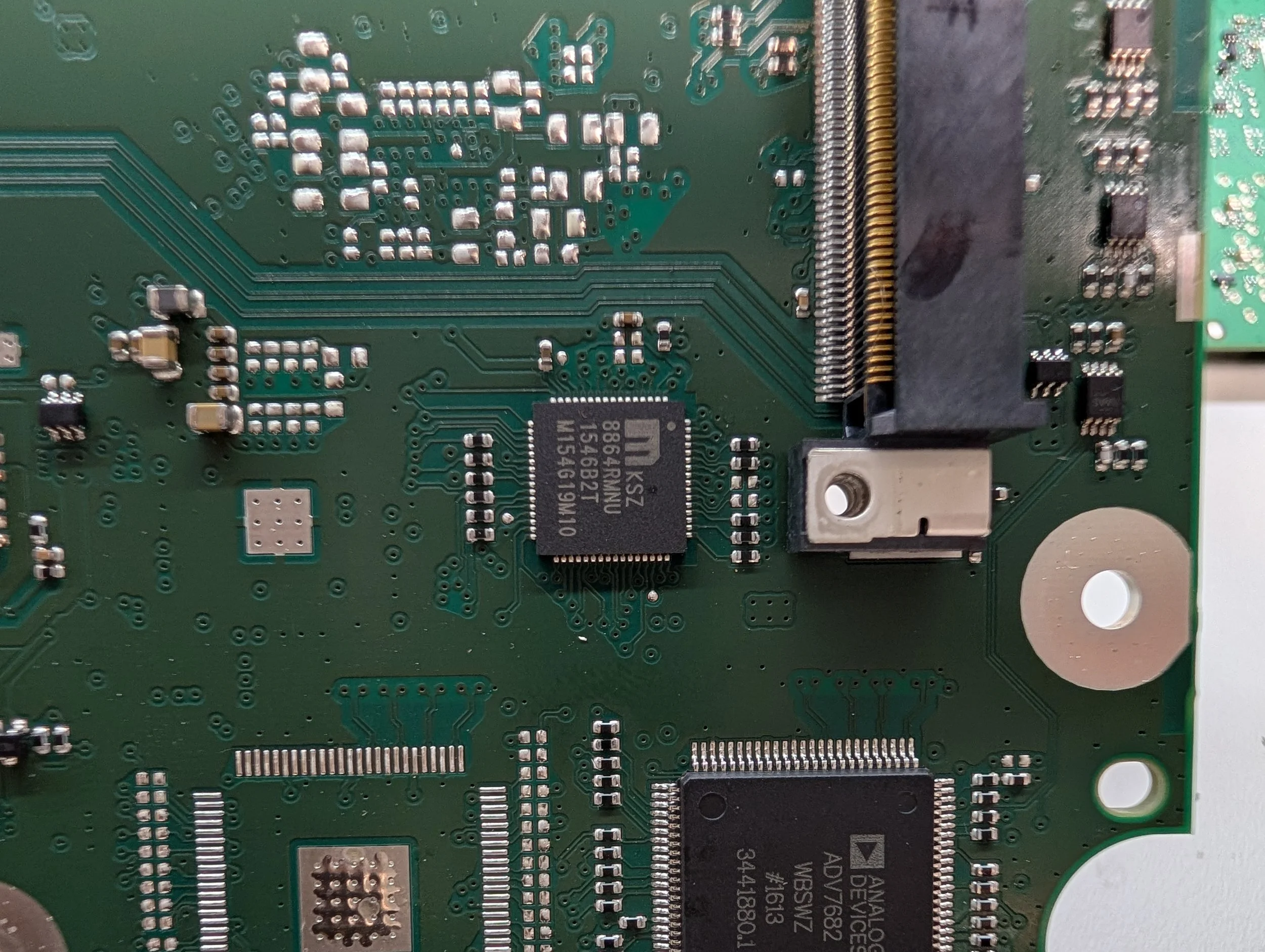
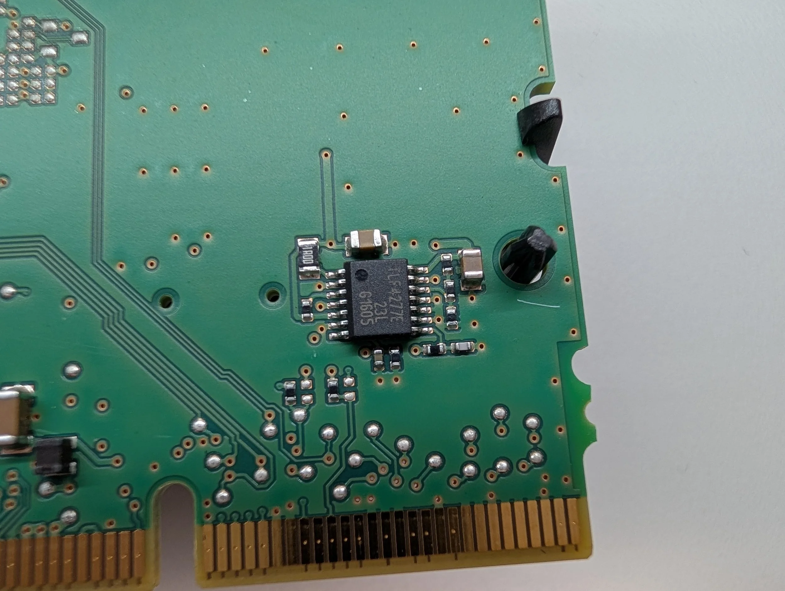
Layer 0 PCB
A top-down view of the Layer 0 PCB.
Board Markings: B140_4110 2747588 27BF
The “Layer 0” PCB is what I’ve nicknamed the lower PCB in the NBT EVO. This unit sits underneath the Layer 1 PCB, and is connected to it via two large connectors in the center of the board.
The Layer 0 PCB acts much like the “motherboard” of the unit. The RF card slots into a PCIe-like slot on this board, as seen on the lower left side. The CD/HDD board plugs into a connector at the very bottom. This PCB allows for the interconnection of much of the device’s RF, video, WiFi, Bluetooth, and Ethernet functionality with the main OMAP processor, located on a daughter board on the underside.
(Also, please excuse the chunk hanging off of my RF Card slot, lol - I’m not sure what happened! It was like that when I popped the lid off the unit. I wonder if it came from a crashed vehicle?)


Oh, one other quick side note - before disassembling, there was also a black plastic reinforcement frame that sat on top of the Layer 0 PCB, providing extra support between it and the Layer 1 PCB. I just didn’t include it in the first photo so it would be easier to see all of the ICs :)
Major Components - Layer 0 PCB (Top side)

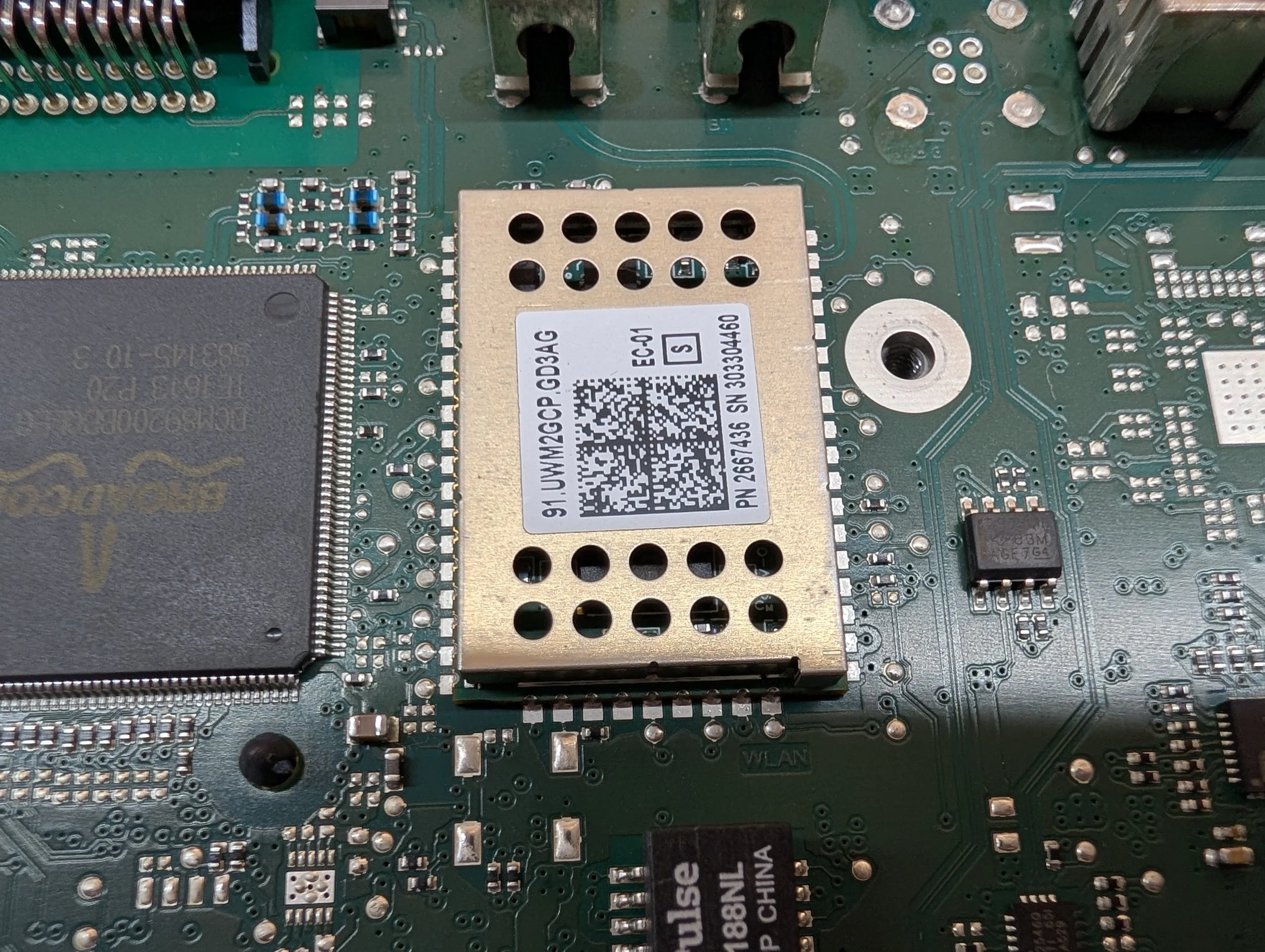


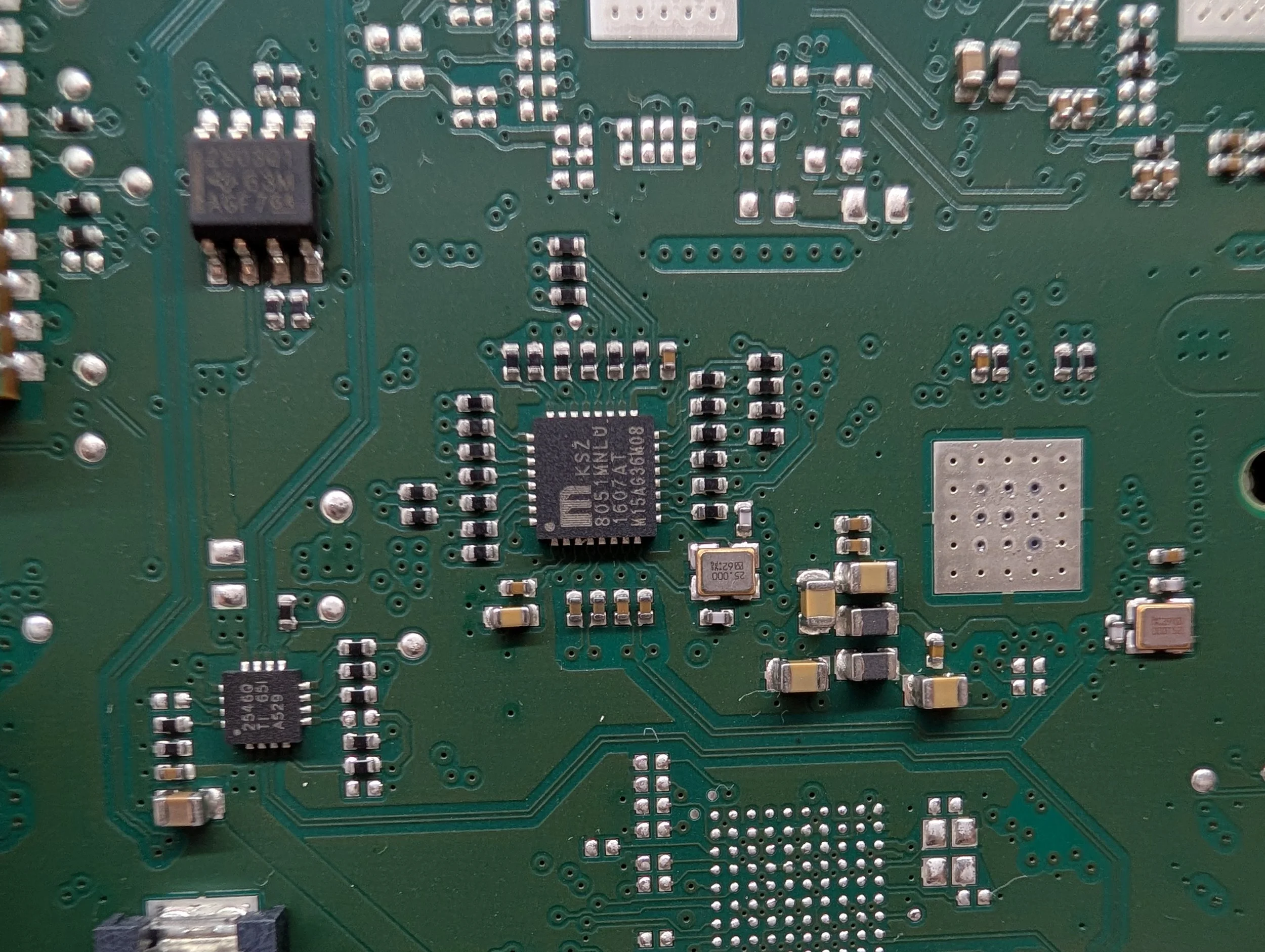

Pulse Electronics Ethernet Transformer/Choke (datasheet)
HX1188NL 1611-PP CHINA
Marvell WiFi & Bluetooth SoC
91.UWM2GCP.GD3AG
PN 2667436 SN 303304460
(I need to pop the top on this to get the exact model, sorry - but I believe it’s based on the Marvell 88W8787 IC)
Broadcom 4-Port Integrated BroadR-Reach Automotive Switch (datasheet)
BCM89200BBQLEG
TE1613 P20 583145-10 3
Micron 1GB SDRAM (datasheet)
6FM17 D9RZZ
MT47H64M16NF-25E AIT:M
Microchip 10Base-T/100Base-TX Automotive Transceiver (datasheet)
KSZ 8051MNLU 1607AT M15A636M08
TI TPS2546-Q1 USB Charging Port Controller (datasheet)
2546Q TI 65I A529
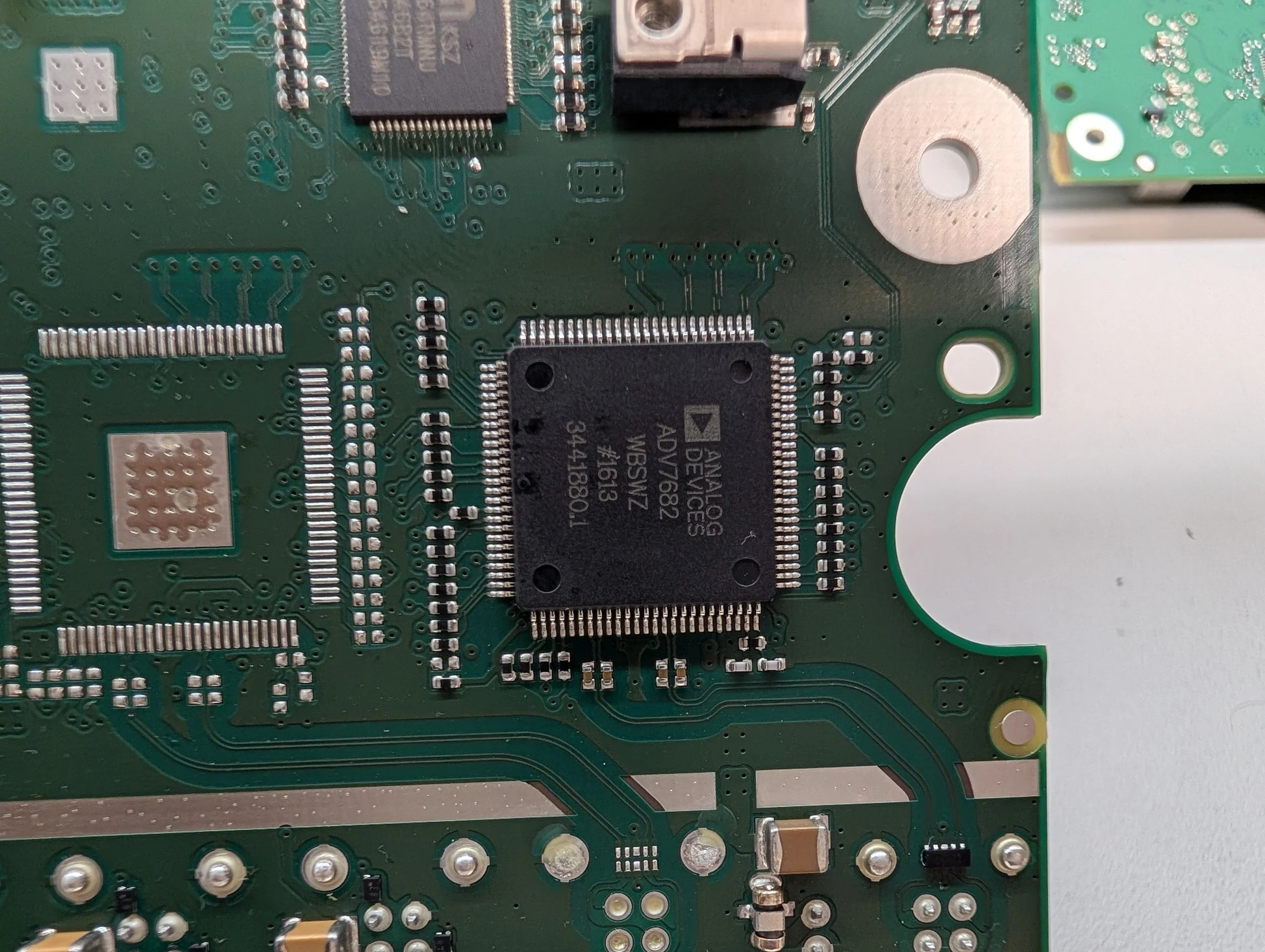
The Underside of Layer 0
The Layer 0 PCB as viewed from the underside, showing the TI OMAP daughter board mounted in the upper right.
Next, the underside of Layer 0! This board has quite a bit going on.
First and foremost, you can see the daughter board mounted to the upper right of the PCB. This board contains the entire OMAP application processor, RAM, and eMMC storage as a removable module.
With the daughter board removed, the layout of the Layer 0 PCB is a bit easier to see.
On the left side of the PCB sits the main IC of the Layer 0 PCB - the TI Jacinto5. There’s 1GB of Micron RAM above, and 1GB of NOR flash to the right. The right side of the board holds another Microchip Ethernet switch, and an Analog Devices video decoder under that - likely for the APIX connection.
Major Components - Layer 0 PCB (Underside)
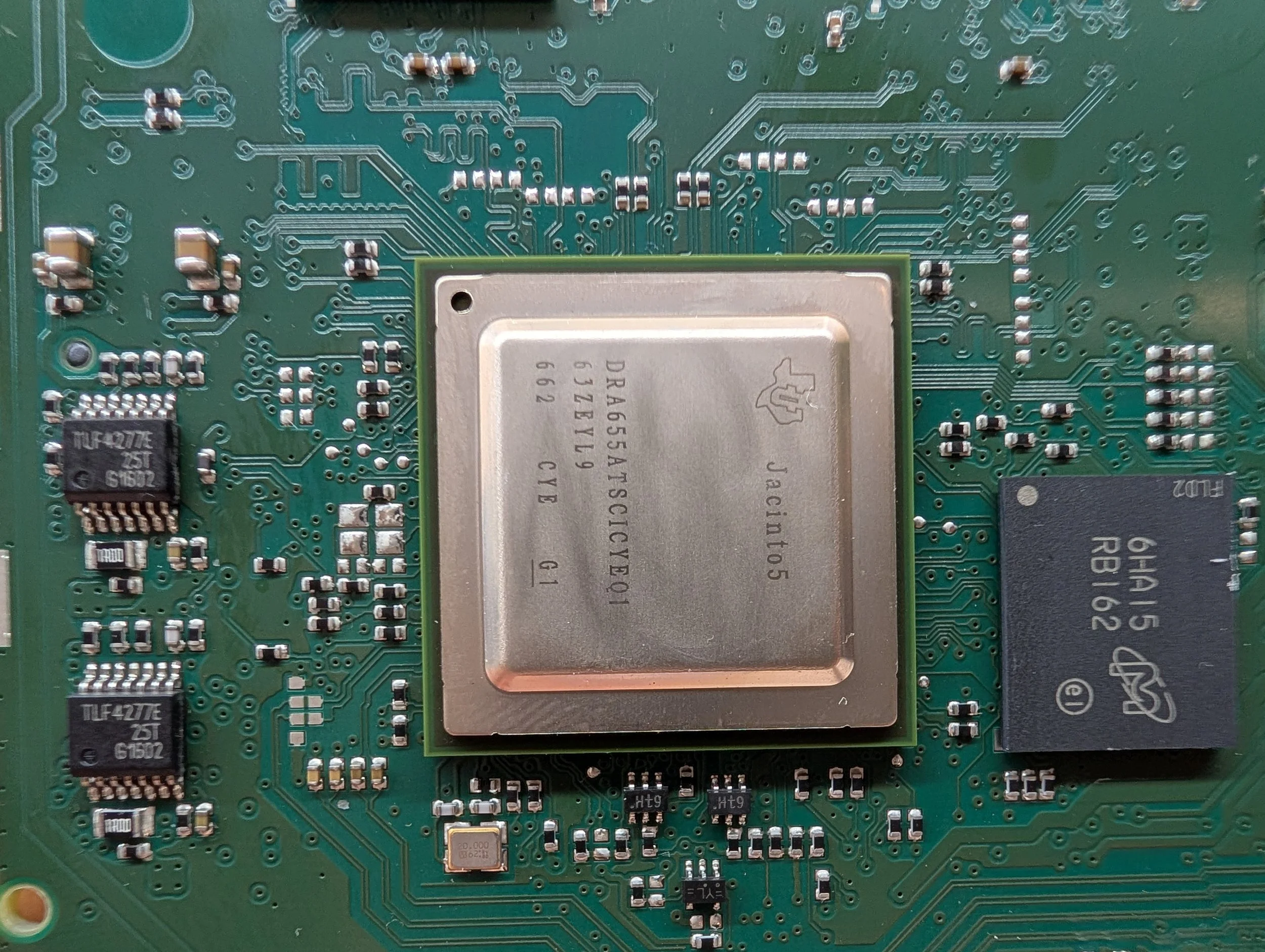
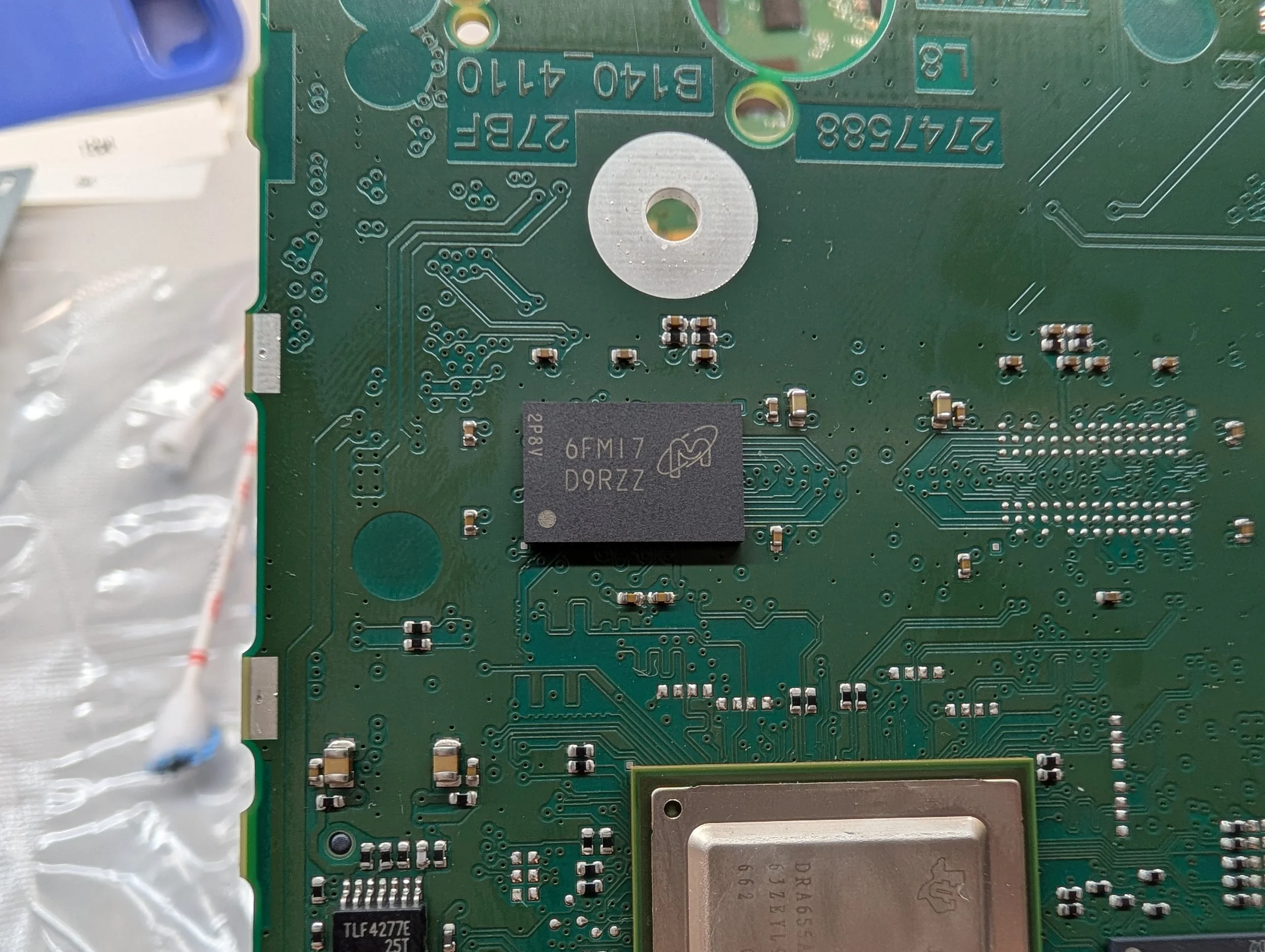
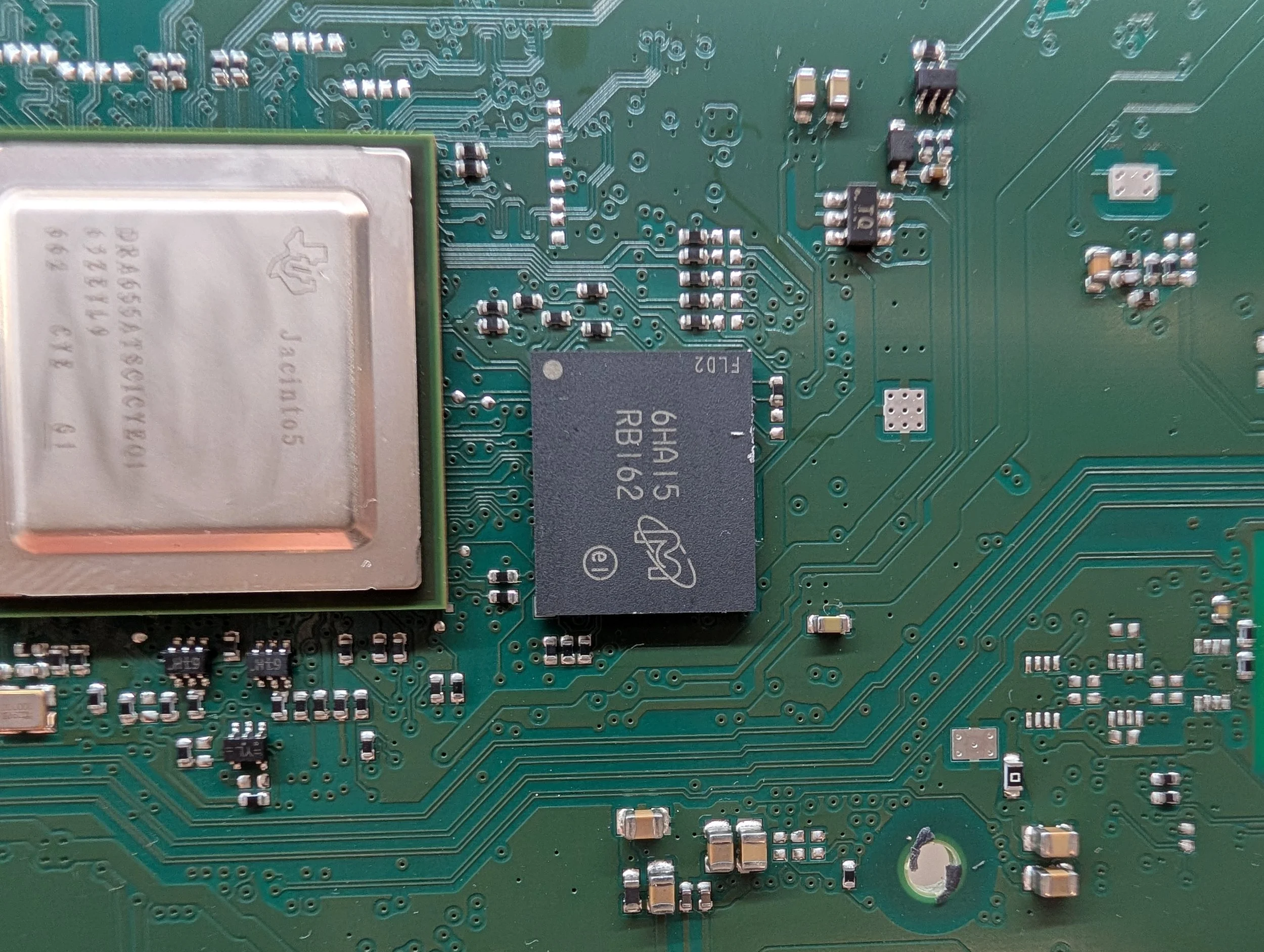
Texas Instruments Jacinto5 Automotive Applications Processor (datasheet)
DRA655ATSCICYEQ1
63ZEYL9 662 CYE G1
Micron 1Gb DRAM (datasheet)
6FM17 D9RZZ
MT47H64M16NF-25E AIT:M
Micron 1Gb NOR Flash (datasheet)
6HA15 RB162
MT28FW01GABA1LPC-0AAT
Microchip 4-Port 10/100 Managed Ethernet Switch with Dual MACs (datasheet)
KSZ 8864RMNU 1546B2T M154G19M10
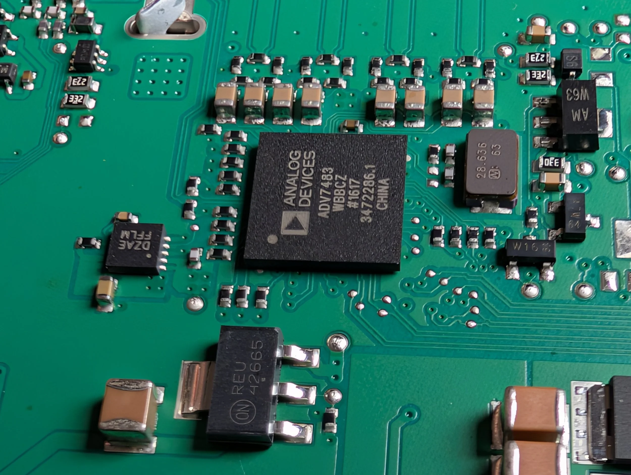
Analog Devices APIX2 Transmitter with Dual Port HDMI and HDCP Support (datasheet)
ADV7682 WBSWZ #1613 3441880.1
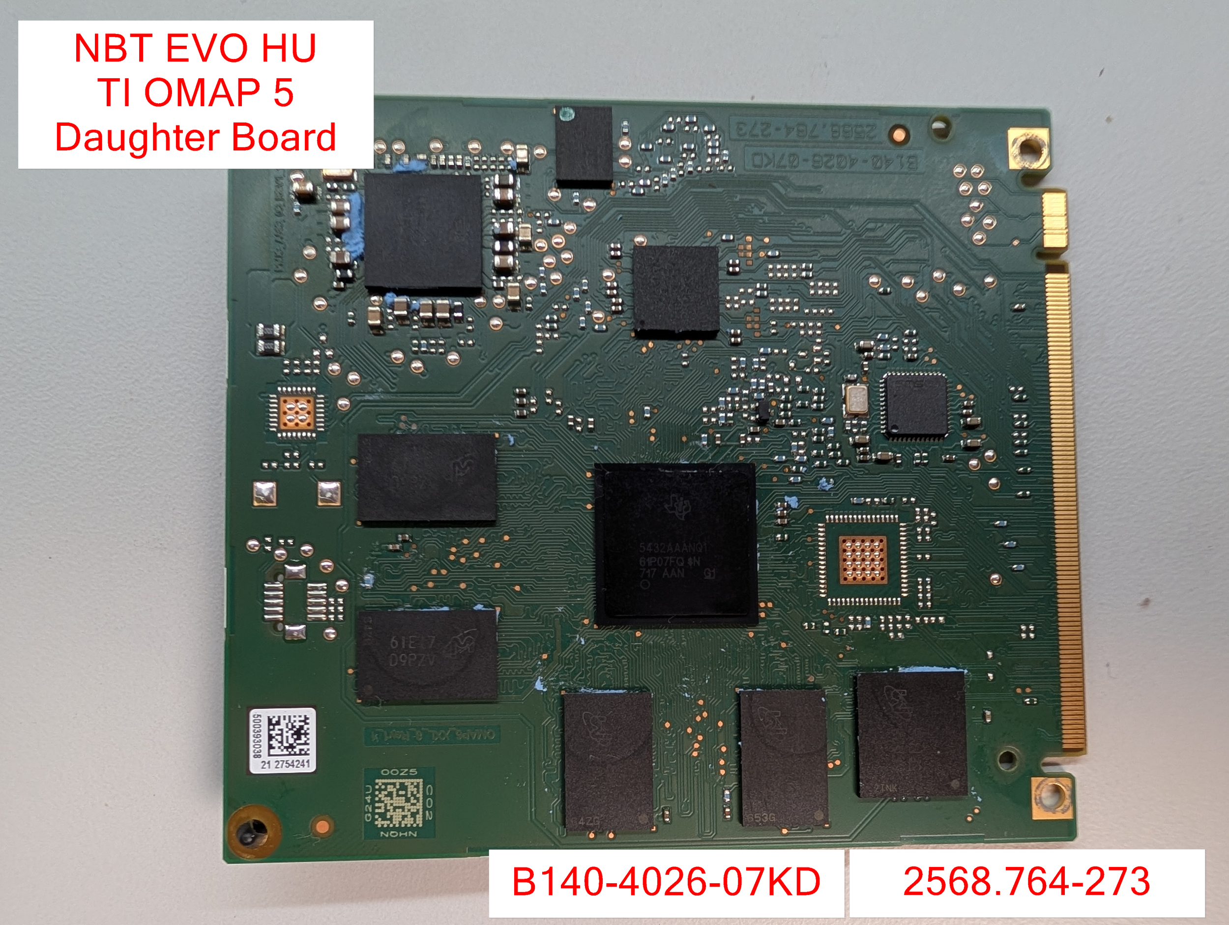
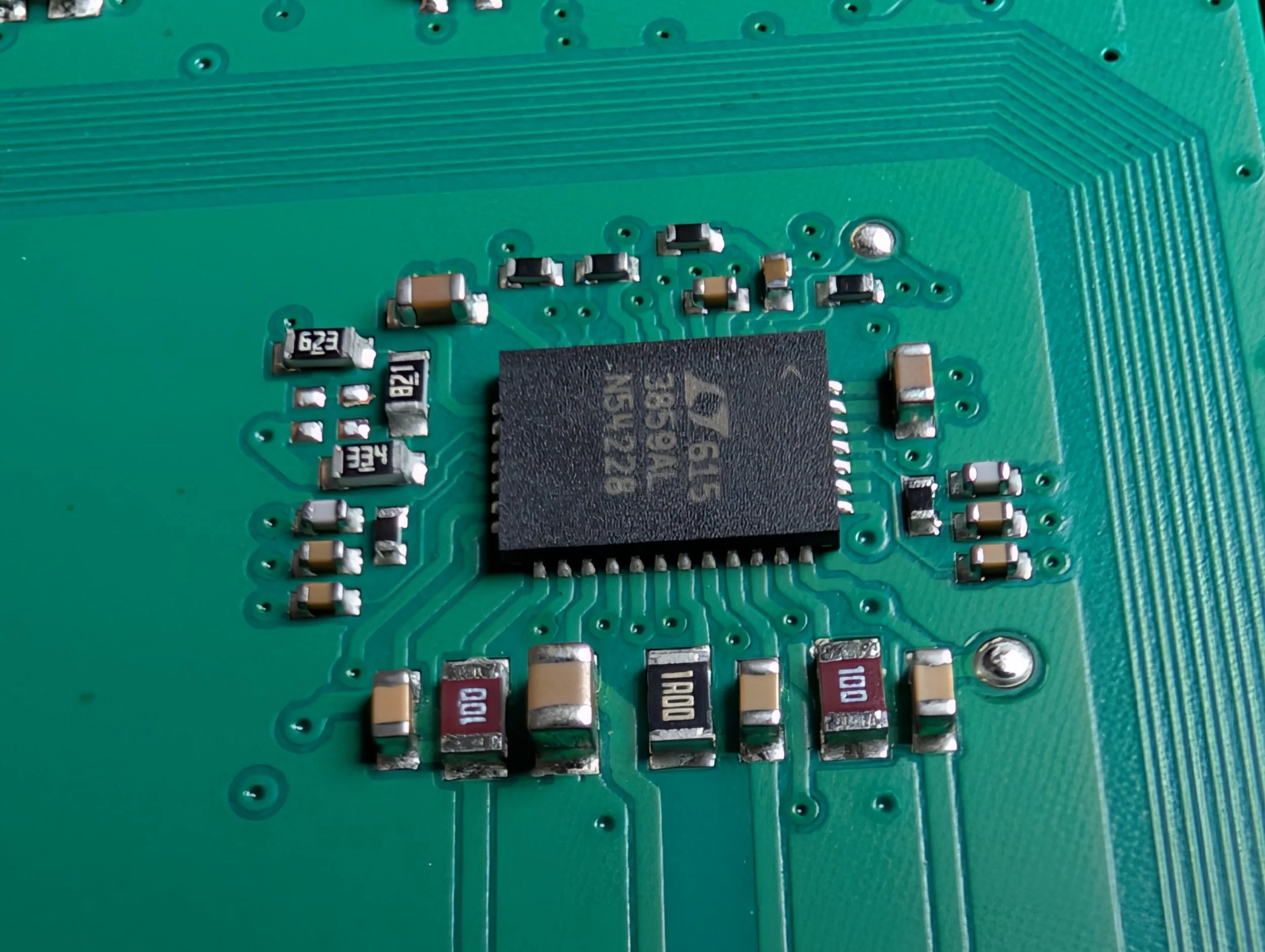
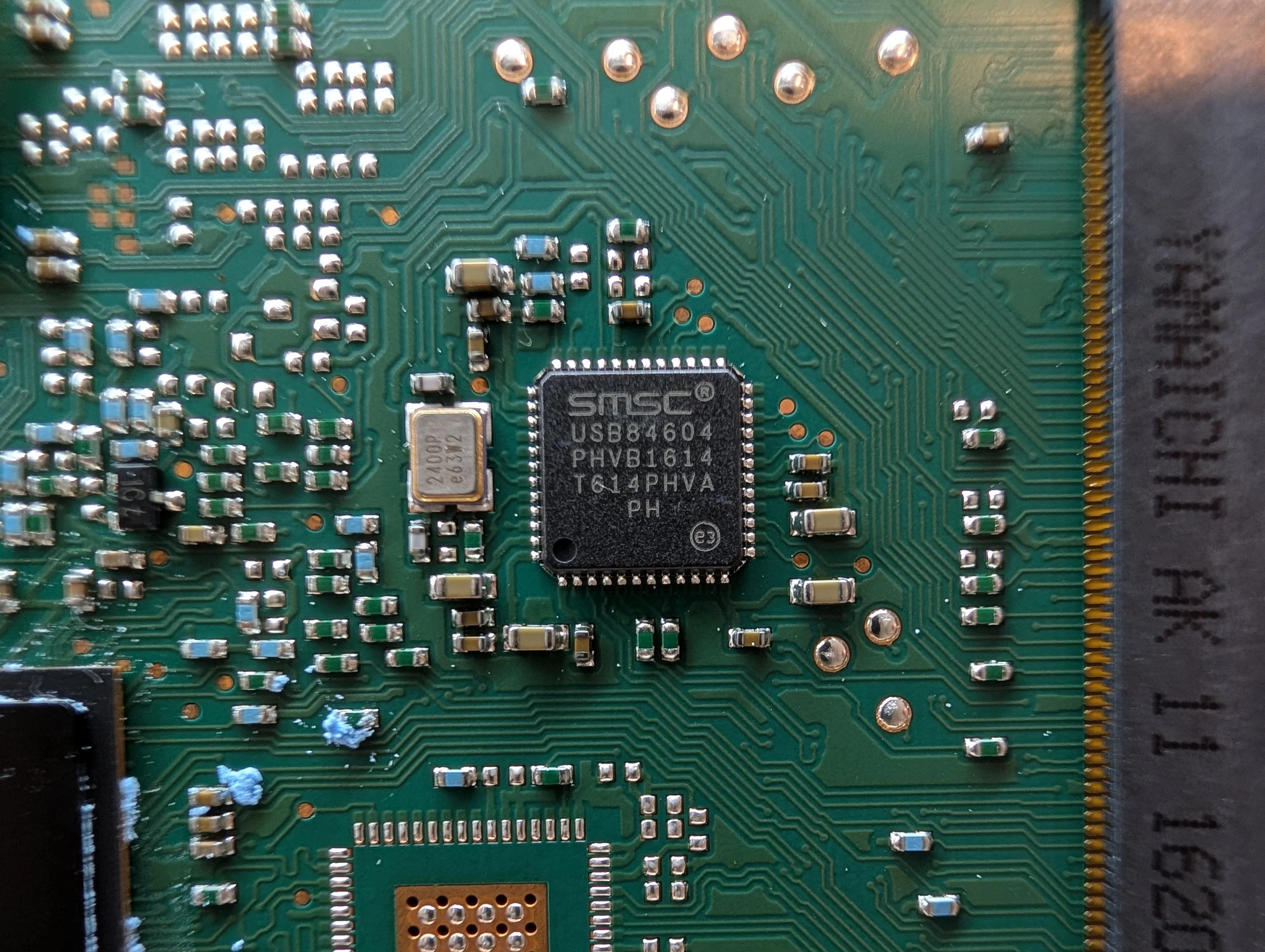
TI OMAP Daughter Board PCB
Board Markings: B140-4026-07KD 2568.764-273
Secondary Marking: OMAP5_XXL_8_Rev1_1
The TI OMAP daughter board is the most compute-heavy processor in the entire module. While I’m unsure what it’s called internally at Harman, I’d personally consider this to be the main “Application Processor”.
The board is designed around the Texas Instruments OMAP5432 processor, a high performance automotive “multimedia processor”. It has two ARM Cortex-A15 cores, two ARM Cortex-M4 cores, and a whole host of other features.
It’s flanked by 2GB of RAM - 1Gb on the front and 1Gb on the back, split into 256Mb modules (newer units got 4GB). Next to that, another Micron chip holding 64Gbit of eMMC flash.
Major Components - OMAP Daughter Board PCB (Top Side)
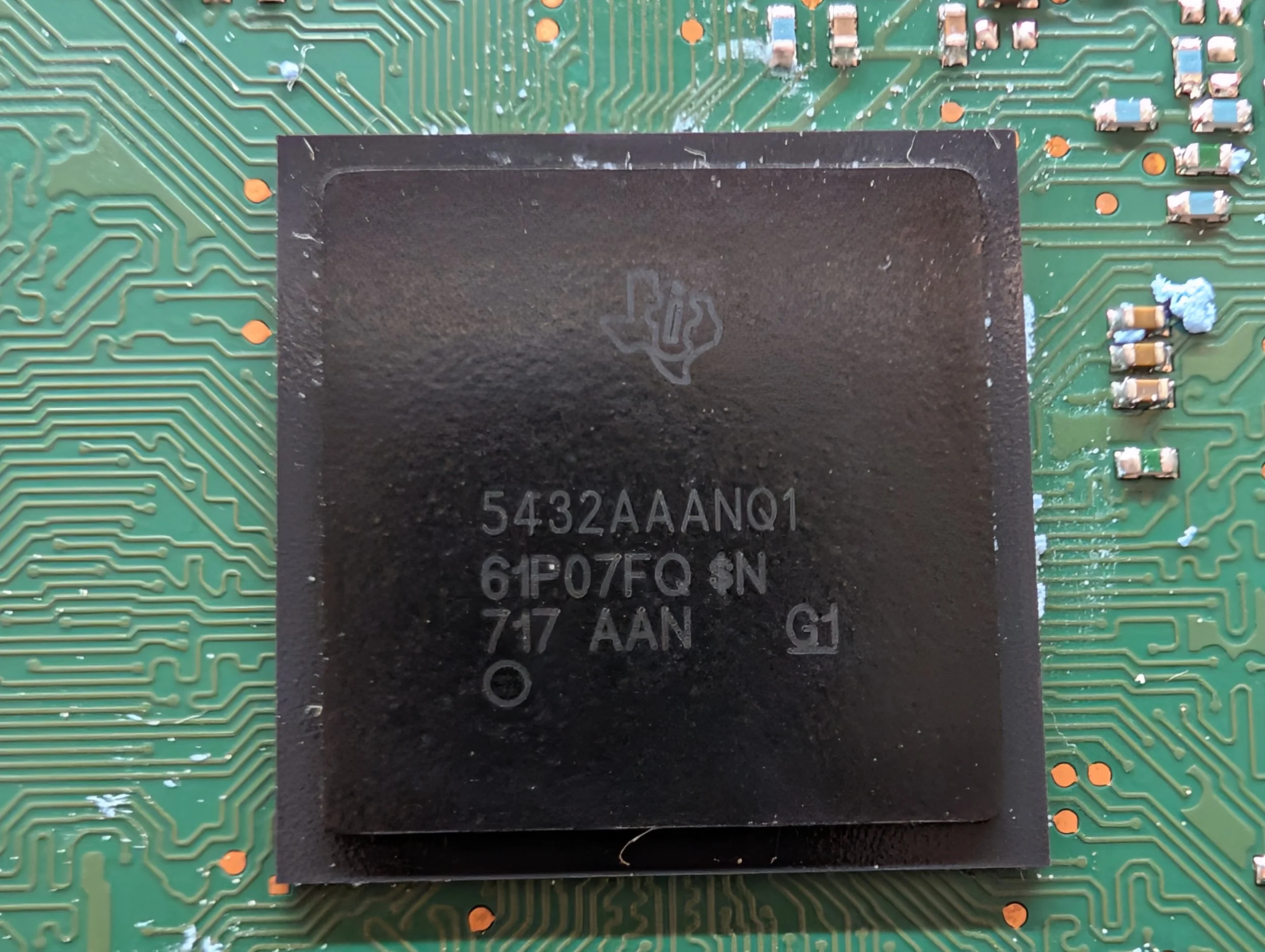


Texas Instruments OMAP5432 (datasheet-ish)
5432AAANQ1 61P07FQ $N 717 AAN G1
Micron 256Mb DDR3L SDRAM (x4) (datasheet)
61E17 D9PZV
MT41K256M16HA-125 AIT:E
Micron 64Gb EMMC (Digi-Key) (datasheet)
6FA28 SFFMS
MTFC8GACAENS-AIT
Micron 64Mb NOR Flash (datasheet)
25Q064A 13EA0 99 MYS
99609A4000
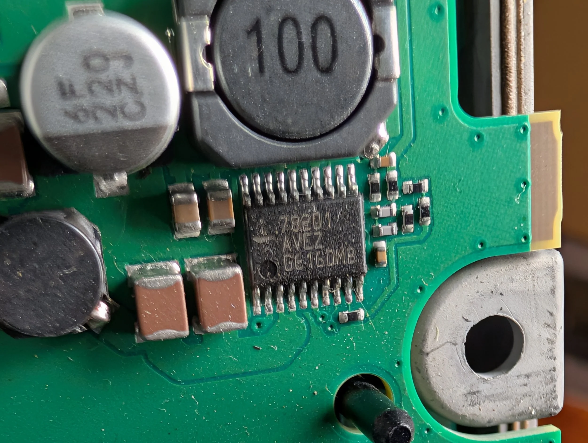
Texas Instruments Power Supply Regulator (datasheet)
TPS659038 OTP 42 1.3 62AHRLW G2 G1
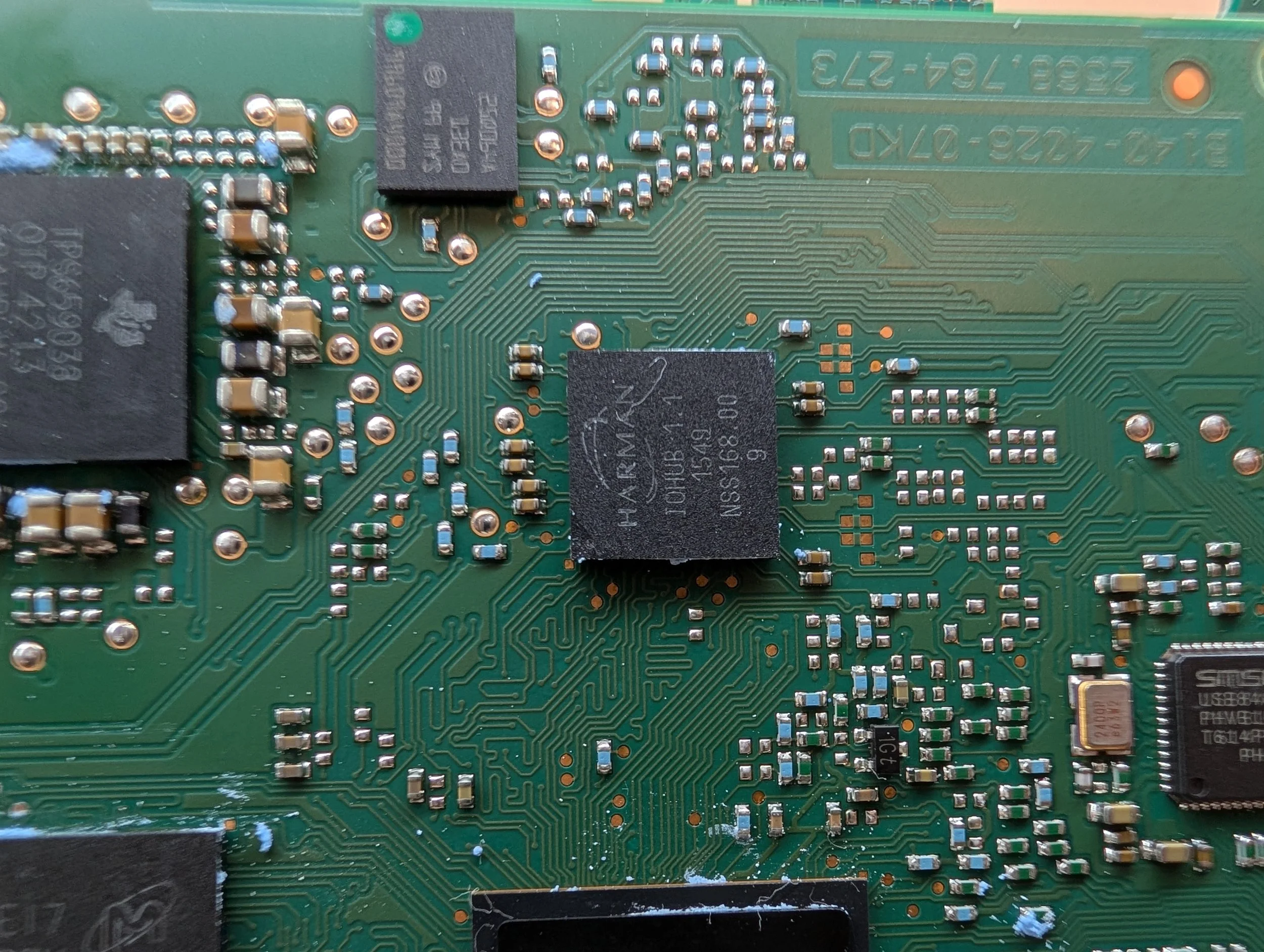
Harman IOHUB (???)
I have no idea what this IC does - something proprietary!
There are a few string references to it in the binary pci-omap543x on the OMAP portion of the device’s filesystem. Will research more.
IOHUB 1.1 1549 NSS168.00 9
SMSC USB 2.0 Hi-Speed 4-Port Controller Hub (datasheet)
USB84604 PHVB1614 T614PHVA PH
The Underside of the OMAP Daughter Board PCB
The underside of the OMAP Daughter Board PCB
The underside of the daughter board PCB is relatively simple, with only a few major components. The other 4x RAM chips (256Mb/ea, another 1GB total), and a PCIe 2.0 Clock Generator.
Major Components - OMAP Daughter Board PCB (Underside)
Micron 256Mb DDR3L SDRAM (x4) (datasheet)
61E17 D9PZV
MT41K256M16HA-125 AIT:E
Diodes Inc PCIe 2.0 Clock Generator (datasheet)
PI6C557-05QLE 1552GC
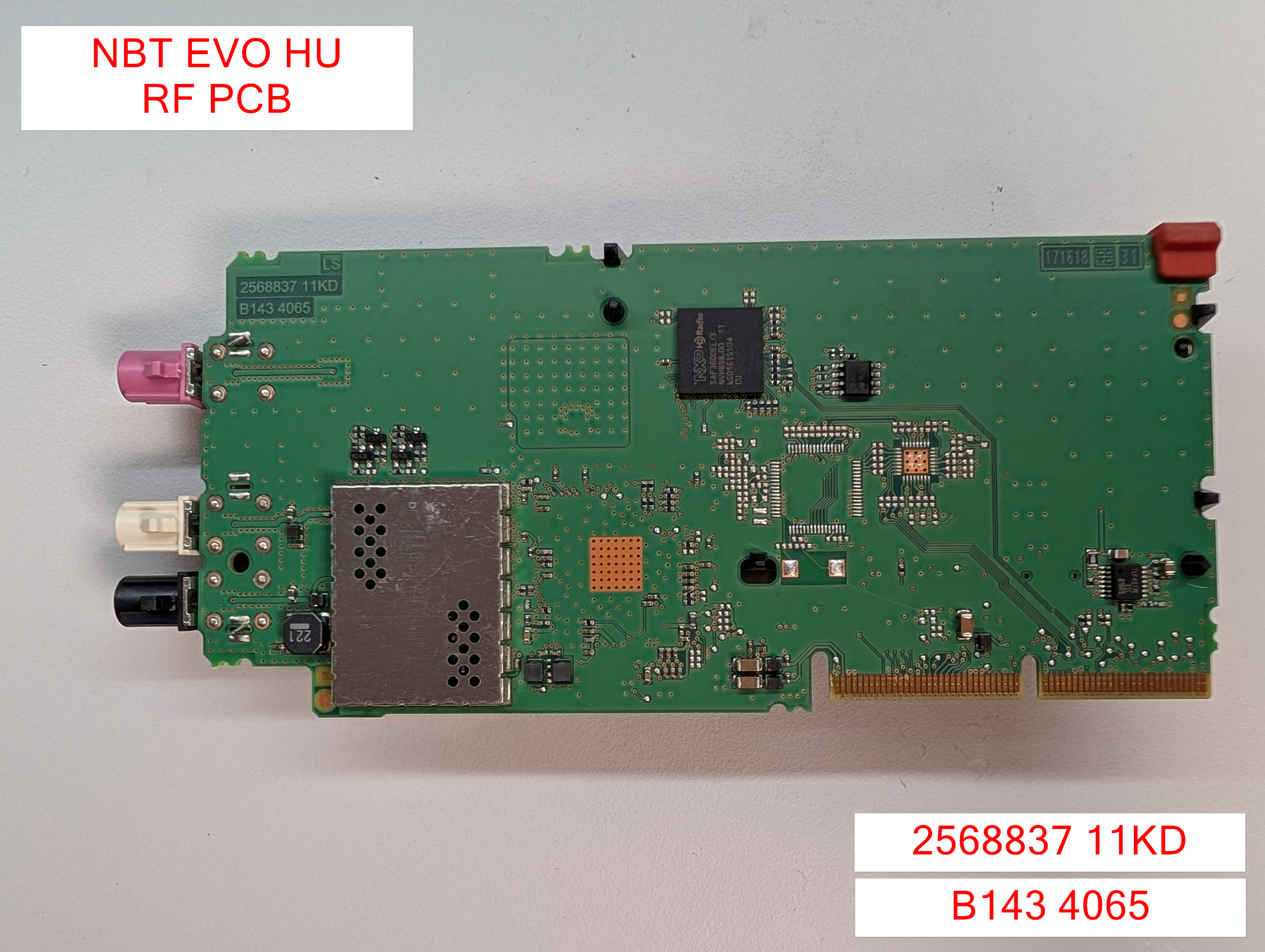
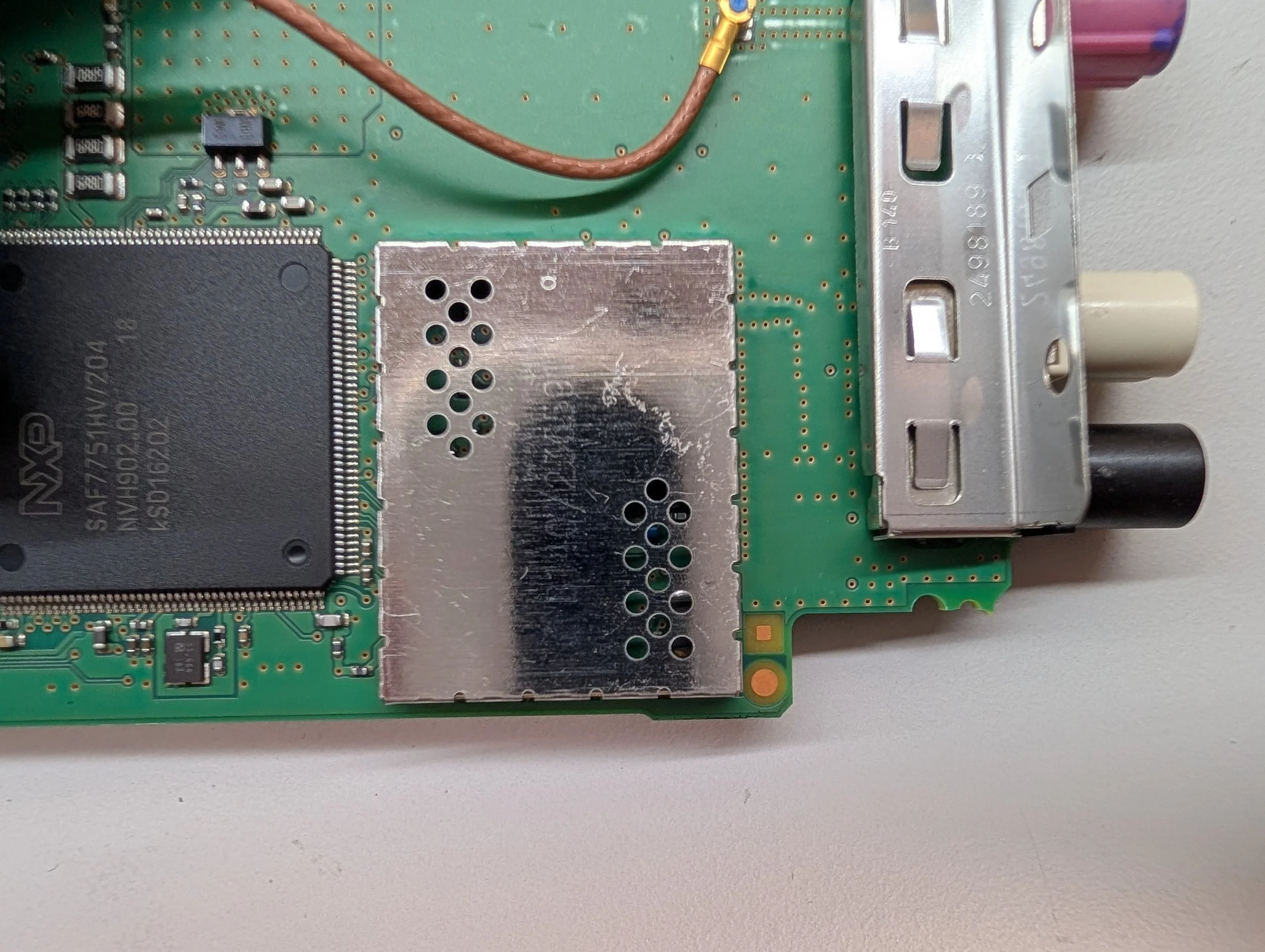
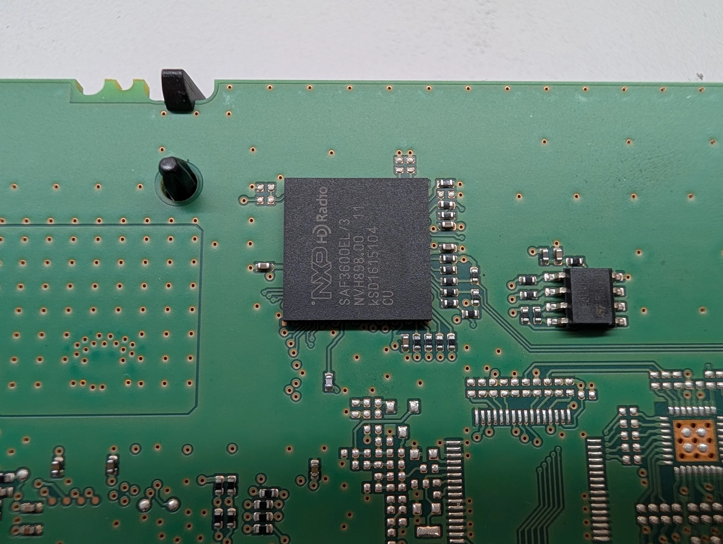
RF PCB
Board Markings: B143 4065 2568837 11KD
Next up, the RF PCB. It holds a majority of the Radio Frequency (RF) interfaces for the device. On this particular model, it has AM radio, FM radio, and SDARS (Satellite Radio).
The exposed Satellite Radio module label.
The large black cover can pop off this PCB, exposing the metal-encapsulated satellite radio module.
Major Components - RF PCB (Font Side)


Satellite Radio Module
P/N: 91.UMS6EMH.G19FAQAG
HWID: B1H4D4C019G
P/N: 2791501
EC-Index: 10
PSN: UAP1G26000AAC01
6H2BMHBW0102000HM8M1XXX
SX-2140-0058-02 L3 16-03-22
NXP High Performance AM/FM/DAB Dual Tuner (datasheet)
SAF7751HV/204
NVH902.00 18 kSD16202
Shielded Mystery IC
I’ll be totally honest: I was rushing with the RF card, and forgot to pop the covers off of these ICs. If it’s been a week and I haven’t updated the post yet, feel free to yell at me - I’ll go disassemble the unit again and take pictures of these.
RF PCB - Back Side
The back side of the NBT EVO’s RF PCB card.
The back side of the board is somewhat similar to the front - not much to see! An NXP Digital Radio processor, some SPI flash memory, an antenna power supply, and another mystery IC (to add to the TODO list…).
Major Components - RF PCB (Back Side)


The “front” of the HDD/CD PCB (there’s not really a clear “front” or “back”, idk)
Board Markings: B140 9049 20FF 2837625
The final PCB in the system, the HDD/CD connectivity PCB! This has three connectors:
One connector to attach to the Layer 0 PCB
One connector to attach to the installed HDD
One connector to attach to the CD/DVD Drive
The “back” of the HDD/CD PCB.
Conclusion
Well, that wraps up my teardown of the BMW/Harman NBT EVO HU infotainment unit!
Unfortunately, not all NBT EVO’s are made equal - being an early unit, this teardown is only a snapshot in time of what the insides of these units can look like. Newer units may be a fair bit different! Always best to do as much research as possible.
If you have any questions about the device or any of the PCBs, feel free to reach out - I’ll try to answer them or update the post as best as I can.
As always, thank you for reading, and happy hacking! (It’s actually December as I’m writing this - so Hacky Holidays!)
Appendix
The appendix contains all of the miscellaneous text and raw data that I didn’t want to clutter the blog post with. I’m hoping including it here makes the data easier to reference/find/grep through/etc.
Yellow Heading Color: #ffd300
Being Pedantic: NBT EVO Model Names
Throughout this article, I’ve referred to this unit as the “NBT EVO HU”. But there’s a secondary important designation: “B211”.
In most of the original NBT EVO FCC filings, IC naming, etc. they seem to have called this unit the “B140” - but there are way more variants than that.
B140 was the initial version of the head unit sold in Europe, but the US got:
B143
B203
B211 (the subject of this teardown)
B212
B247
B359
To be entirely honest, I don’t know what all of the variant differences are yet! Some shipped with different versions of iDrive, some had different size screens, there are all sorts of variations. I just wanted to put this out there so people are aware that the contents of this teardown (which focused on a B211 unit) may be different from other variants, other regions, etc.
Decoding Micron Part Numbers
As always, dealing with Micron ICs that have short, un-Googleable markings can be a pain! You can use Micron’s own website to decode the “FBGA” code marked on the part.
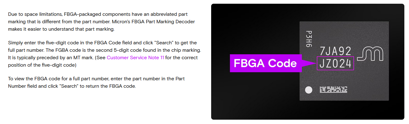
I spy with my little eye, a typo…
Also, funny side note: Can you spot the typo on their own site? (Hint: They accidentally spell it “FGBA” once)
NBT EVO Top Label - Text Dump
The top label of the unit contained the following text. Note: As I’ve written it, it roughly goes top-to-bottom, left-to-right. I left out the FCC compliance (not ID), Dolby, and SiriusXM portions because they’re long and not that interesting.
Manufactured by: Harman Infotainment
Model: NBT EVO HU

CLASS 1 LASER PRODUCT
DIN EN 60825-1:2008-05

12V - 12A

FCC ID: T8GB140
IC: 6434A-B140

MSIP-CMM-T8G-NBTevoHU
CMMIT ID: 2014DJ5625
IFT: RCPBMNB15-110

QD ID: 59940

2505754

N1374

NTC Type Approved
No: ESD-1510161C

TRA
REGISTERED No: ER36109/14
DEALER No: 0028019/10

ICASA
TA-2014/2055
APPROVED

CCAK14LP2350T6

R 204-460018

OMAN-TRA
TRA/TA-R/2196/14
13/11/2014

Complies with IDA Standards DB19172
NBT EVO Front Label - Text Dump
The front of the unit contained a small label with the following text:
Manufactured in the USA by: Harman Automotive

B211305G3229764

Model No.: HB B211 EC: 305
100991 10
HW: 3.2
SNR: 3080889

Type: NBT HU EVO
MAC-Adr: a056b28c24c3
BT-Adr: a056b2335496
Accession No.: 1331416-000
Version: US
Date: 29/16

BMW 6512
CI244897201
NBT EVO CD Drive Label - Text Dump
The sticker on the top side of the unit’s disk drive contained the following text:
24331014181
000102644061
DV68V110
TL0100141818
NBT EVO Part Numbers & Mfg Dates
This list only covers the B211 model of unit. Data courtesy of RealOEM.com
65125B52189 (07/01/2024 - )
65125A28B06 (11/01/2021 - )
65125A472B5 (03/01/2021 - 08/26/2022)
65125A41A09 (03/01/2021 - 04/08/2021)
65125A24047 (07/01/2020 - 01/21/2021)
65125A0C479 (03/01/2020 - 04/10/2021)
65125A08175 (11/01/2019 - 03/02/2020)
65129824994 (07/01/2019 - 11/12/2019)
65129877384 (03/01/2019 - 07/10/2019)
65129437960 (11/01/2018 - 08/20/2019)
65128732663 (11/01/2018 - 10/15/2018)
65128736173 (07/01/2018 - 12/06/2018)
65128721893 (03/01/2018 - 08/01/2018)
65128718155 (03/01/2018 - 04/28/2018)
65128707199 (03/01/2018 - 02/20/2018)
65128708268 (11/01/2017 - 01/21/2023)
65128804468 (07/01/2017 - 12/17/2020)
65128800158 (07/01/2017 - 07/19/2017)
65128796226 (07/01/2017 - 05/31/2017)
65128794123 (03/01/2017 - 07/01/2017)
65128780777 (11/01/2016 - 01/21/2023)
65129867504 (08/01/2016 - 11/01/2016)
65122448972 (07/01/2016 - 08/25/2016) (The teardown unit)
65126833452 (03/01/2016 - 07/20/2016)